
Quick Answer: When evaluating hdi pcb vs standard pcb, a standard board relies on mechanical drilling with an 8-mil minimum via size, while an HDI board utilizes 4-mil laser-drilled microvias to support fine-pitch BGAs. Although an HDI PCB costs 30% to 50% more per square inch due to sequential lamination, switching from an 8-layer standard board to a compact 4-layer HDI board can actually reduce your total bare board cost by 15% through material reduction. Key takeaways:
- Mechanical drills cannot reliably route BGA components with a pitch below 0.5mm without massive DFM failures.
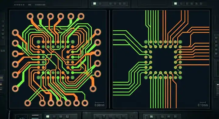
- HDI laser microvias save up to 40% of routing space, allowing you to drastically shrink the overall board size.
- Reducing your total layer count offsets the manufacturing premium you pay for laser drilling.
- Microvias placed directly in BGA pads require epoxy fill and capping (VIPPO) to prevent assembly solder voids.
Table of Contents
- What Is the Core Difference Between HDI and Standard PCBs?
- How Does HDI PCB vs Standard PCB Cost Actually Compare?
- When Must You Abandon Standard PCBs for HDI?
- Can Switching to HDI Actually Save You Money?
- How Does HDI vs Standard PCB Affect Your Production Lead Time?
- Why Is HDI Better for High-Speed Signal Integrity?
- What Are the Most Common HDI Design Mistakes?
- How Do You Ensure a Reliable PCBA Process for HDI?
- FAQ
You spent three weeks carefully routing a dense 8-layer board, only for the manufacturer to put your order on hold because your mechanical vias are too close together. They advise you to upgrade the design, but your purchasing department is screaming about the 40% price jump. Sound familiar? After processing over 5,000 dense multi-layer orders last year, we constantly see hardware engineers trying to force high-density processors onto legacy manufacturing processes. Here is exactly how to compare an hdi pcb vs standard pcb — and why upgrading might actually shrink your final invoice.
What Is the Core Difference Between HDI and Standard PCBs?
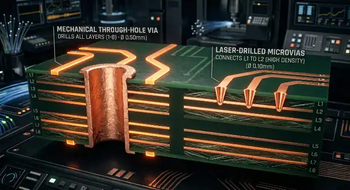
Standard PCBs rely on mechanical drill bits that top out around 0.15mm (6 mils) and go completely through all layers, while HDI (High-Density Interconnect) PCBs utilize precision lasers to ablate tiny 0.1mm (4 mils) microvias that only connect adjacent layers. This fundamental shift from full-depth mechanical drilling to layer-by-layer laser ablation defines the entire technology gap.
Here’s where it gets real…
On forums like r/PrintedCircuitBoard, beginners often think HDI just means “smaller trace widths.” It actually refers to sequential lamination. A standard board is pressed together all at once and drilled. An HDI PCB (like a 1+4+1 stack-up) is built by pressing the core, laser drilling it, plating it, adding another outer layer, pressing it again, and laser drilling again. This takes significantly more time on the factory floor.
- Standard via pads consume massive amounts of routing space on every single layer they pass through.
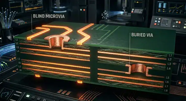
- Laser microvias are blind or buried, freeing up physical space on the layers they do not touch.
- HDI enables via-in-pad technology, allowing you to place components incredibly close together.
How Does HDI PCB vs Standard PCB Cost Actually Compare?
An HDI PCB typically costs 30% to 50% more per square inch than a standard PCB due to the expensive laser drilling time, specialized thin prepregs, and multiple sequential lamination press cycles. For a standard 100x100mm prototype batch, a standard 6-layer board might cost $150, whereas a 6-layer HDI (1+4+1) board will jump to roughly $280 to $350.
So what does this actually mean for your budget?
Engineers look at that per-board premium and immediately run away. But you cannot evaluate these technologies based on a 1-to-1 footprint comparison. You pay the premium specifically so you can shrink the physical footprint of your hardware.
| Manufacturing Feature | Standard PCB | HDI PCB (1+N+1) | Cost Impact |
|---|---|---|---|
| Drilling Method | Mechanical Drill (0.15mm min) | Laser Ablation (0.075mm min) | HDI is 3x more expensive to drill. |
| Lamination Cycles | 1 Cycle | 2+ Cycles | HDI adds 2 to 4 days to lead time. |
| Via Placement | Through-hole (wastes space) | Blind/Buried & Via-in-Pad | HDI saves up to 40% board space. |
| Setup Fee (NRE) | Low ($100 – $150) | High ($250 – $400+) | HDI hurts small prototype runs more. |
Upload your BOM and Gerbers today for a free DFM review. Our engineering team will calculate exact quotes for both technologies.
When Must You Abandon Standard PCBs for HDI?
You must abandon standard PCBs and switch to HDI the moment you select a BGA (Ball Grid Array) component with a pitch of 0.4mm or smaller, or when your routing density leaves you with less than 0.05mm of clearance between pads. Mechanical drill bits physically cannot fit between the pads of a 0.4mm BGA without violating the factory’s minimum annular ring limits.
Now, here’s the part that surprises most customers…
We see engineers on StackExchange trying to invent crazy “dog-bone” fanout patterns to make a dense processor work on standard FR4. They submit the Gerbers, and our automated CAM software rejects it instantly. To make a 0.15mm mechanical drill work reliably, you need a 0.35mm copper pad. At a 0.4mm pitch, you only have 0.05mm of electrical clearance left, guaranteeing a short circuit during etching.
- 0.8mm BGA pitch: Easily routed on a standard PCB using mechanical vias.
- 0.5mm BGA pitch: Requires strict DFM, borderline for standard boards, better with HDI.
- 0.4mm BGA pitch: Absolutely mandates HDI laser microvias and via-in-pad routing.
Can Switching to HDI Actually Save You Money?
Yes, switching to HDI saves you money when the high routing density allows you to reduce your overall layer count from 8 layers down to 4 layers, or shrink your total board dimensions by more than 30%. The cost savings from using significantly less raw FR4 material and eliminating inner copper layers completely offsets the premium you pay for the laser drilling process.
Want the honest answer?
If your board is mostly simple components with one tiny BGA, paying for sequential lamination is a waste of money. But if you have multiple dense processors, forcing them onto a standard board requires adding more and more signal layers just to escape the chips.
- Standard 8-layer board (100x100mm) = High cost due to layer count and size.
- HDI 4-layer board (60x60mm) = Lower total material cost, faster SMT assembly.
- Fewer overall layers also mean fewer chances for impedance mismatches on your high-speed data lines.
How Does HDI vs Standard PCB Affect Your Production Lead Time?
A standard multi-layer PCB takes roughly 5 to 7 days to manufacture, while an HDI PCB adds 2 to 3 days to your timeline for every sequential lamination cycle required, pushing the average lead time to 12 to 18 days. Every time an outer microvia layer is added, the factory must completely repeat the pressing, laser drilling, and plating processes.
Here’s the thing…
Hardware managers often assume an HDI board is just a regular board with smaller holes, and they demand standard turnaround times. We constantly have startups begging us to expedite a 2+4+2 HDI board in 5 days. It is physically impossible. The epoxy resins need time to cure, and the plasma desmear process cannot be rushed without destroying the via’s structural reliability.
- Standard 6-layer board: 1 lamination cycle = Fully compatible with quick-turn PCB prototyping.
- HDI 1+4+1 board: 2 lamination cycles = Minimum 10 to 12 days bare board fabrication.
- HDI 2+4+2 board: 3 lamination cycles = Minimum 15+ days bare board fabrication.
Why Is HDI Better for High-Speed Signal Integrity?
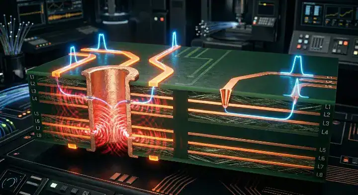
HDI technology drastically improves signal integrity by replacing standard through-hole vias with laser microvias, completely eliminating the unused “via stubs” that cause severe signal reflections at speeds above 3GHz. If you are routing PCIe Gen 4, USB 4.0, or high-speed telecom PCB data links, standard via stubs act like tiny antennas that radiate EMI and corrupt your digital data.
The real question is…
Why spend weeks tuning your differential pairs if you are going to destroy the impedance with a mechanical via? When a high-speed signal drops from Layer 1 to Layer 3 through a standard drill hole, the remaining metal pipe hanging down to Layer 8 acts as a resonant stub. Laser microvias only connect Layer 1 to Layer 2, leaving the transmission line perfectly clean.
- Standard Via: Creates parasitic capacitance and signal reflections due to leftover stubs.
- Microvia: Only spans the required layers, creating a clean, short transmission path.
- Via-in-Pad: Eliminates the need for escape traces, significantly reducing power plane inductance.
What Are the Most Common HDI Design Mistakes?
The most frequent HDI design mistake is stacking microvias directly on top of each other across three or more layers without using solid copper fill, causing extreme thermal stress and microscopic via fractures during the hot assembly reflow process. Another major error involves specifying microvias but ignoring the 1:1 aspect ratio limit of the laser drill.
But here’s what most guides won’t tell you…
How do you prevent your expensive prototype from failing in the field? Veteran engineers constantly warn about reliability issues in HDI stack-ups. We see this daily: customers submit stacked vias to save a millimeter of space. We mandate staggering them like a staircase because un-filled stacked vias trap air, which violently expands in our reflow ovens and literally blows the copper plating apart.
| Design Feature | Red Flag (High Failure Risk) | Green Flag (Reliable Factory Yield) |
|---|---|---|
| Via Arrangement | Stacking 3+ microvias vertically. | Staggering microvias step-by-step. |
| Aspect Ratio | Laser drilling a 4-mil hole through 6-mil prepreg. | Keeping dielectric thickness below 4 mils for a 4-mil drill. |
| BGA Routing | Leaving via-in-pad holes open and unfilled. | Specifying VIPPO (Via-in-Pad Plated Over) on the drawing. |
Check out our guide on how to optimize microvias before you finalize your layout.
How Do You Ensure a Reliable PCBA Process for HDI?
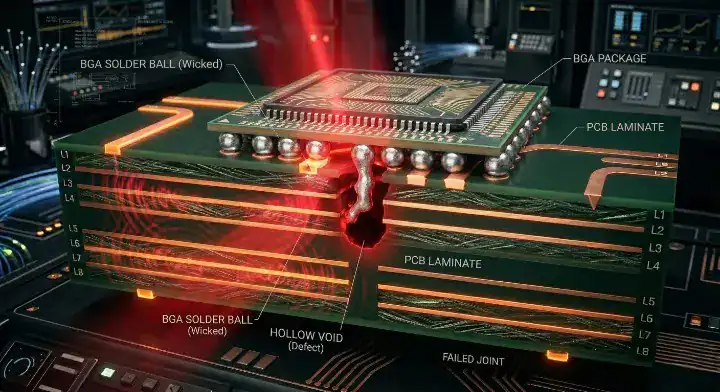
You ensure reliable HDI assembly by requesting via-in-pad plated over (VIPPO) technology, which fills the laser microvias with epoxy and plates them flat with copper, preventing your expensive solder paste from wicking down the hole and starving the joint. Without VIPPO, your high-end processor will disconnect from the board during standard field use.
Now, here’s the part that surprises most customers…
A perfectly fabricated bare HDI board will still fail if your assembly house uses outdated equipment. The passive components used on HDI boards are microscopic (often 0201 or 01005 packages). If your EMS partner uses an old pick-and-place machine, the placement accuracy will not be tight enough. At QueenEMS, we run strict 3D AOI and X-Ray inspection on every single BGA assembly to guarantee zero solder bridging.
- VIPPO keeps your BGA pads perfectly flat for reliable stencil printing.
- Advanced X-Ray inspection is mandatory to check for voids under high-density chips.
- Partnering with a single factory for fabrication and assembly eliminates finger-pointing if a board fails.
FAQ
What does a 1+N+1 stack-up actually mean in HDI? The “N” represents the standard mechanically drilled core of the board, while the numbers on the outside represent the sequentially laminated HDI microvia layers. A 1+4+1 board has a 4-layer core with one layer of microvias laser-drilled onto the top and one on the bottom, resulting in a 6-layer total board. A 2+4+2 would be an 8-layer board requiring three total press cycles.
Can I mix mechanical vias and laser microvias on the same board? Yes, every HDI board mixes both technologies. You use tiny laser microvias for the outer high-density layers (like Layer 1 to 2) to escape your BGAs, and you use standard mechanical drills for the through-holes that connect top-to-bottom for power and ground. Upload your Gerbers to let our CAM engineers verify your drill file setup.
Is it harder to repair or rework an HDI PCB? Yes, it is significantly harder. Because the traces are usually 3 mils or smaller and the BGAs are tightly packed, manual soldering iron rework is almost impossible without damaging adjacent components. You must use a highly precise BGA rework station with localized hot air.
Written by the QueenEMS Engineering Team. Ready to build your next board? Contact us today at QueenEMS.