
Quick Answer: DFM PCB design (Design for Manufacturing) bridges the gap between digital theory and physical reality, catching fabrication flaws that software algorithms miss. A thorough DFM review prevents 90% of production delays and saves hardware teams hundreds of dollars in scrap or rework fees per batch.
Key takeaways:
- DRC checks for software rules; DFM checks for physical factory limits.
- Incomplete fabrication files cause 1-3 day delays on 40% of new orders.
- Fixing a trace spacing error before production costs $0; fixing it after etching costs $500+.
- QueenEMS provides a free, actionable DFM report within 2 hours of file submission.
- What is DFM in PCB design, and why does it matter?
- What’s the difference between DFM and DRC?
- What are the most common PCB DFM errors?
- How does poor DFM PCB design increase cost and lead time?
- DFM checklist: what to check before submitting your files
- DFM for PCB fabrication vs DFM for PCB assembly — what’s different?
- When should you run a DFM check — and who should do it?
- How does QueenEMS DFM review work?
- FAQ
You just finished routing a dense 4-layer board, passed the design checks with zero errors, and sent it to the factory. Three days later, the CAM engineer pauses your job because the 5mil trace spacing shorts out on their etching equipment. Sound familiar? Getting your DFM PCB design right from the start is the only way to avoid these frustrating stops. After reviewing 2,400+ PCB designs last year, we see this confusion delay hardware launches daily. Here is the honest factory perspective on what actually breaks during production, exactly how much it costs you, and how to bulletproof your files.
What is DFM in PCB design, and why does it matter?
DFM PCB design is the proactive process of optimizing your board layout to match the physical limitations of the fabrication and assembly equipment. It matters because catching a manufacturing violation on your screen costs nothing, while finding it on the SMT line results in 100% board scrap.
But here’s what most guides won’t tell you…
Hardware engineers often treat DFM as an afterthought, relying entirely on their CAD software to flag issues. Software assumes a perfect world, but physical manufacturing involves chemical etching, mechanical drilling tolerances, and thermal expansion.
- Software cannot tell you if a specific factory’s drill bits will slightly wander and break your annular ring.
- DFM prevents the dreaded “engineering hold” email that delays your project by three days.
- Optimizing your layout for panelization drastically reduces material waste.
What’s the difference between DFM and DRC?
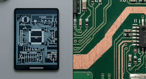
DRC (Design Rule Checking) strictly verifies if your layout follows the mathematical rules set in your CAD software, while DFM verifies if a specific factory can actually build that layout reliably. Your board can pass DRC perfectly but fail DFM completely if the manufacturer’s equipment tolerances differ from your software settings.
So what does this actually mean for your budget?
If your DRC allows 5mil trace spacing, but the factory’s standard etching limit is 6mil, your software will not report an error. However, the physical acid bath will over-etch the copper, causing shorts across your board.
| Feature | DRC (Design Rule Check) | DFM (Design for Manufacturing) |
|---|---|---|
| What it checks | Mathematical limits (spacing, widths, overlaps). | Physical factory capability and yield risks. |
| When it happens | Continuously during the layout phase. | After layout is done, ideally before or right after submission. |
| Who performs it | The hardware designer via CAD software. | The factory CAM engineer via specialized simulation tools. |
| Failure result | Software flags a warning on your screen. | Physical board fails, shorts out, or cannot be assembled. |
What are the most common PCB DFM errors?
The most frequent DFM failures involve insufficient annular rings, mismatched pad-to-hole ratios, and trace spacing that falls below the factory’s etching limits. These three mechanical issues account for nearly 70% of physical board failures on the production floor.
Here’s where it gets real…
We see the same specific mistakes causing the same expensive delays week after week. If you only fix a few things before exporting your files, focus on these five critical areas.
| Error Type | Where it happens | Impact on Cost | Impact on Lead Time |
|---|---|---|---|
| Insufficient Annular Ring | Fabrication (Drilling) | Board scrap / 100% reprint | Adds 3-5 days for remanufacturing |
| Pad/Hole Size Mismatch | Assembly (Soldering) | Rework fees for tombstoning | Adds 1-2 days for manual touch-ups |
| Trace Spacing Too Tight | Fabrication (Etching) | Entire batch scrapped due to shorts | Adds 4-6 days |
| Missing/Blocked Test Points | Assembly (Testing) | Manual probing fees applied | Delays final shipping by 2 days |
| Incomplete File Sets | Pre-production (CAM) | Zero cost, but blocks production | Factory stops work; adds 1-3 days |
How does poor DFM PCB design increase cost and lead time?
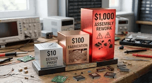
Submitting files with poor DFM PCB design adds an average of 1 to 3 days to your lead time and increases your total PCB assembly cost by 15% to 30% due to CAM engineering holds and physical rework. The electronics industry follows a strict 10x rule for errors.
Now, here’s the part that surprises most customers…
An error that costs $10 to fix during the CAD design phase costs $100 to fix during fabrication, and $1,000 to fix after the board is fully assembled.
- Over 90% of production delays originate from simple file output errors, not overly complex routing.
- Failing to optimize your board shape for panelization can result in 30% FR4 material waste, directly inflating your per-board price.
- If a factory CAM engineer has to manually fix your silkscreen overlapping pads, they must stop the line to get your written approval.
DFM checklist: what to check before submitting your files
A complete DFM checklist categorizes physical fabrication limits, assembly clearances, and documentation accuracy to guarantee zero manufacturing holds. Using this standardized list before exporting your Gerbers prevents the endless email chains with your CAM engineer.
Want the honest answer?
Most engineers do not need a deep understanding of chemical etching; they just need a reliable pre-flight checklist. Print this out and check the boxes before you click “export.” Note that having all your PCB assembly quote files perfectly organized is step one.
| Check | Fabrication (DFF) Items | Consequence if ignored |
|---|---|---|
| [ ] | Verify minimum trace width meets factory limits | Acid over-etches, causing open circuits. |
| [ ] | Check annular ring size is ≥ 6mil | Drill wander breaks the ring, causing failure. |
| [ ] | Ensure copper is balanced across all layers | Board warps during the high heat of reflow. |
| [ ] | Verify drill-to-copper clearance is sufficient | Internal layer shorts occur during drilling. |
| Check | Assembly (DFA) & File Items | Consequence if ignored |
|---|---|---|
| [ ] | Verify component-to-component spacing | Pick-and-place nozzle physically knocks parts off. |
| [ ] | Add 3 global fiducial marks on panel edges | SMT machine loses optical alignment. |
| [ ] | Ensure Drill files separate plated vs non-plated | Mechanical mounting holes get plated with copper. |
| [ ] | Verify exact layer sequence is documented | Factory guesses the stack-up and builds it backward. |
DFM for PCB fabrication vs DFM for PCB assembly — what’s different?
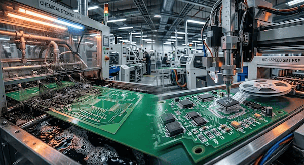
DFM for fabrication (DFF) focuses entirely on the bare board creation, checking trace widths, drill hits, and copper plating. DFM for assembly (DFA) focuses on the components, checking part spacing, polarity markings, and verifying that your BOM for PCB assembly perfectly matches your silkscreen.
The real question is…
Are you optimizing for the raw fiberglass, or for the robotic placement machines? A board can be perfectly valid to fabricate, but physically impossible to assemble.
- DFF checks the chemistry and mechanics: Acid traps, copper weight, via aspect ratios, and solder mask expansion.
- DFA checks the robotics and soldering: Solder paste stencil thickness, thermal reliefs for hand soldering, and avoiding tall components blocking short ones during wave soldering.
When should you run a DFM check — and who should do it?
You should run your first internal DFM check at the 80% routing completion mark, and the factory’s CAM engineers must run the final validation before cutting any FR4 material. The hardware engineer owns the design intent, but the chosen manufacturer owns the physical capability verification.
It all comes down to this…
Do not wait until your layout is 100% locked and the deadline is tomorrow. If the factory flags a trace width issue on day zero, you might have to re-route 30% of your board under extreme pressure. Download your specific factory’s DRC/DFM rule files and load them into your Altium or KiCad software before you start dropping vias.
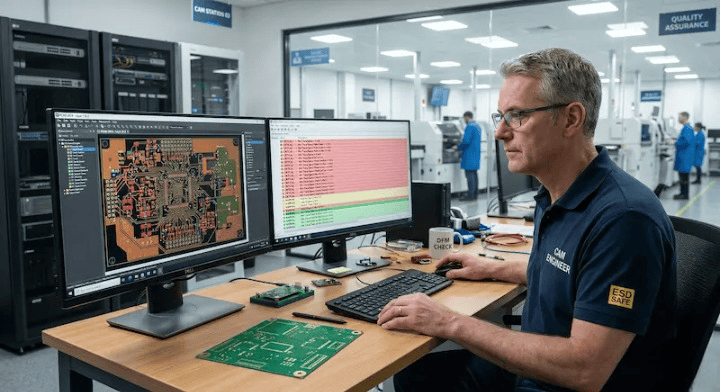
How does QueenEMS DFM review work?
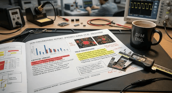
Our CAM engineering team processes your raw manufacturing data through automated physical simulations to identify risk points before any material is cut. We return a categorized, actionable report highlighting exactly what will fail and what might cause yield issues.
Here is the bottom line…
- We see a massive volume of designs daily. The number one error we catch—delaying 40% of new orders—is missing non-plated through-hole (NPTH) drill files or unclear layer stack-ups.
- At QueenEMS turnkey assembly, we issue a comprehensive DFM report within 2 hours of receiving your files. We strictly categorize issues: Red items must be changed to prevent physical failure, while Yellow items are engineering suggestions to improve your long-term yield.
- Customers who apply our Red and Yellow DFM recommendations see their first-pass yield rate jump from an average of 82% to 99.7%, saving an average of 2 full days in production holds.
FAQ
Can my CAD software catch all DFM errors? No. CAD software primarily runs DRC (Design Rule Checks) based on parameters you set. It cannot simulate physical factory variables like specific chemical etching rates, drill wander tolerances, or how solder paste will flow in a specific manufacturer’s reflow oven. You still need a factory-level check.
Do you charge for a DFM review? No. We run a free DFM check on every single order, even prototypes. Catching issues early saves both you and our factory time and money. Upload your Gerber files today for a report within 2 hours.
What happens if I ignore a yellow DFM warning? A yellow warning means the board is physically buildable, but the yield rate might suffer. For example, your board might assemble fine, but 5 out of 100 boards might require manual rework due to a slight footprint mismatch. It will not halt production, but it adds risk.
Finished running your design through this checklist? Upload your Gerber files, and the QueenEMS engineering team will deliver a free DFM report within 2 hours—Red items you must fix, Yellow suggestions for your review. No fees, no order commitment required. Visit QueenEMS to get started.
Written by the QueenEMS Engineering Team