
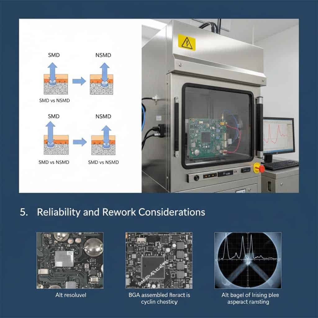
The choice between SMD and NSMD BGA pad designs depends on whether your priority is mechanical bond strength or the precision of the copper land area. This decision fundamentally dictates how your board handles thermal stress and physical drops.
Imagine you’ve just invested thousands in a high-density production run, only to find high failure rates during environmental stress testing. You see cracked solder joints and lifted pads under the microscope, and suddenly, your time-to-market is in jeopardy. This frustration is often the result of choosing the wrong pad geometry for your specific application’s thermal and mechanical demands. By mastering the differences between Solder Mask Defined (SMD) and Non-Solder Mask Defined (NSMD) pads, you can ensure high-reliability performance and seamless manufacturing.
In this guide, we will break down the technical nuances of each Bga pad type to help you make the most informed engineering choice.
Why is BGA pad design critical for assembly?
The Bga pad serves as the foundational interface between the delicate silicon package and the rugged PCB substrate. It must manage the electrical signals while withstanding the physical stresses of thermal expansion and contraction.
How does pad geometry affect reliability?
You need to understand that the geometry of the pad determines the shape and volume of the solder joint. This shape directly influences how stress is distributed throughout the assembly.
- Determines the wetting area for solder.
- Influences the risk of pad cratering.
- Impacts the routing density between pads.
But here is the kicker: even a tiny design variation can lead to massive reliability gaps.
Key Takeaway
Choosing the correct pad design ensures that your BGA PCB assembly survives the harsh realities of the field without premature failure.
| Feature | Impact on Reliability |
| Pad Shape | Dictates stress distribution |
| Solder Volume | Affects fatigue resistance |
| Copper Adhesion | Prevents pad lifting |
Understanding these basics allows you to optimize your board’s lifespan from the very first layer.
What are Solder Mask Defined (SMD) Bga pads?
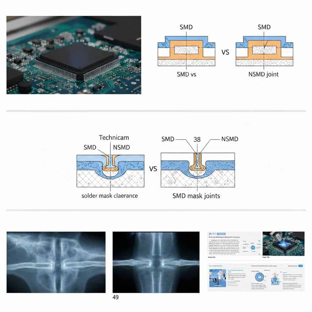
An SMD Bga pad is defined by the solder mask aperture being smaller than the underlying copper pad. This creates a “mask-defined” area where the solder makes contact, essentially overlapping the copper with protective mask material.
Is the SMD design better for mechanical strength?
Yes, the primary advantage is that the mask acts like a physical “anchor” for the copper land. You will find this particularly useful in designs where the pads are prone to lifting under high mechanical stress.
- Increased pad-to-board adhesion strength.
- Better protection against pad cratering.
- Consistent solderable area regardless of copper etch tolerances.
The best part? This design provides a massive safety net for heavy components.
Key Takeaway
Use SMD pads when your product faces extreme vibrations or heavy mechanical handling to prevent the copper from detaching from the laminate.
| Parameter | SMD Characteristic |
| Definition | Mask aperture < Copper pad |
| Bond Strength | Higher (anchored by mask) |
| Routing Space | Lower (larger copper pads) |
This structural integrity makes SMD a favorite for ruggedized industrial electronics.
How do Non-Solder Mask Defined (NSMD) Bga pads work?
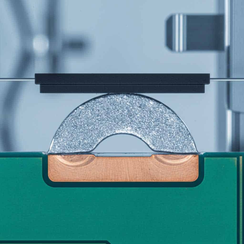
The NSMD Bga pad features a solder mask opening that is larger than the copper land itself. This allows the solder to wrap around the sides of the copper, creating a robust metallurgical bond on both the top and the edges.
Why is NSMD the industry standard for precision?
You will find that NSMD pads offer superior registration because the copper etching process is typically more accurate than the solder mask printing process. This precision is vital for the tight pitches found in modern High-Density PCB Assembly.
- Excellent solder joint fatigue life.
- Lower parasitic capacitance for high-speed signals.
- Maximum clearance for trace routing between pads.
You might be wondering, is it really that much better? In most high-speed and consumer applications, the answer is a resounding yes.
Key Takeaway
NSMD pads provide better thermal fatigue resistance and more routing flexibility, making them the default choice for most small-pitch BGA components.
| Parameter | NSMD Characteristic |
| Definition | Mask aperture > Copper pad |
| Fatigue Life | Higher (side wetting) |
| Precision | Excellent (copper defined) |
The increased flexibility in routing often makes NSMD the only viable choice for complex, multi-layered boards.
Which Bga pad design offers better solder joint reliability?
Solder joint reliability in a Bga pad is measured by how well it resists cracking under thermal cycling and mechanical shock. While NSMD excels in thermal cycling, SMD often wins the battle against physical impact.
How does side-wetting improve fatigue life?
With NSMD, the solder wets the vertical sides of the copper pad, creating a larger surface area for the bond. This extra “grip” allows the joint to flex slightly during thermal expansion without snapping.
- Reduces stress concentration at the pad edge.
- Provides a more flexible interconnection.
- Enhances long-term durability in high-temp environments.
Want to know the secret to longevity? It’s all about letting the joint breathe under stress.
Key Takeaway
If your device operates in environments with frequent temperature swings, NSMD is your best bet for preventing solder fatigue.
| Stress Type | Recommended Pad Design |
| Thermal Cycling | NSMD |
| Physical Drop/Shock | SMD |
| High-Speed Signal | NSMD |
This tradeoff means you must evaluate your product’s end-use case before finalizing your CAD library.
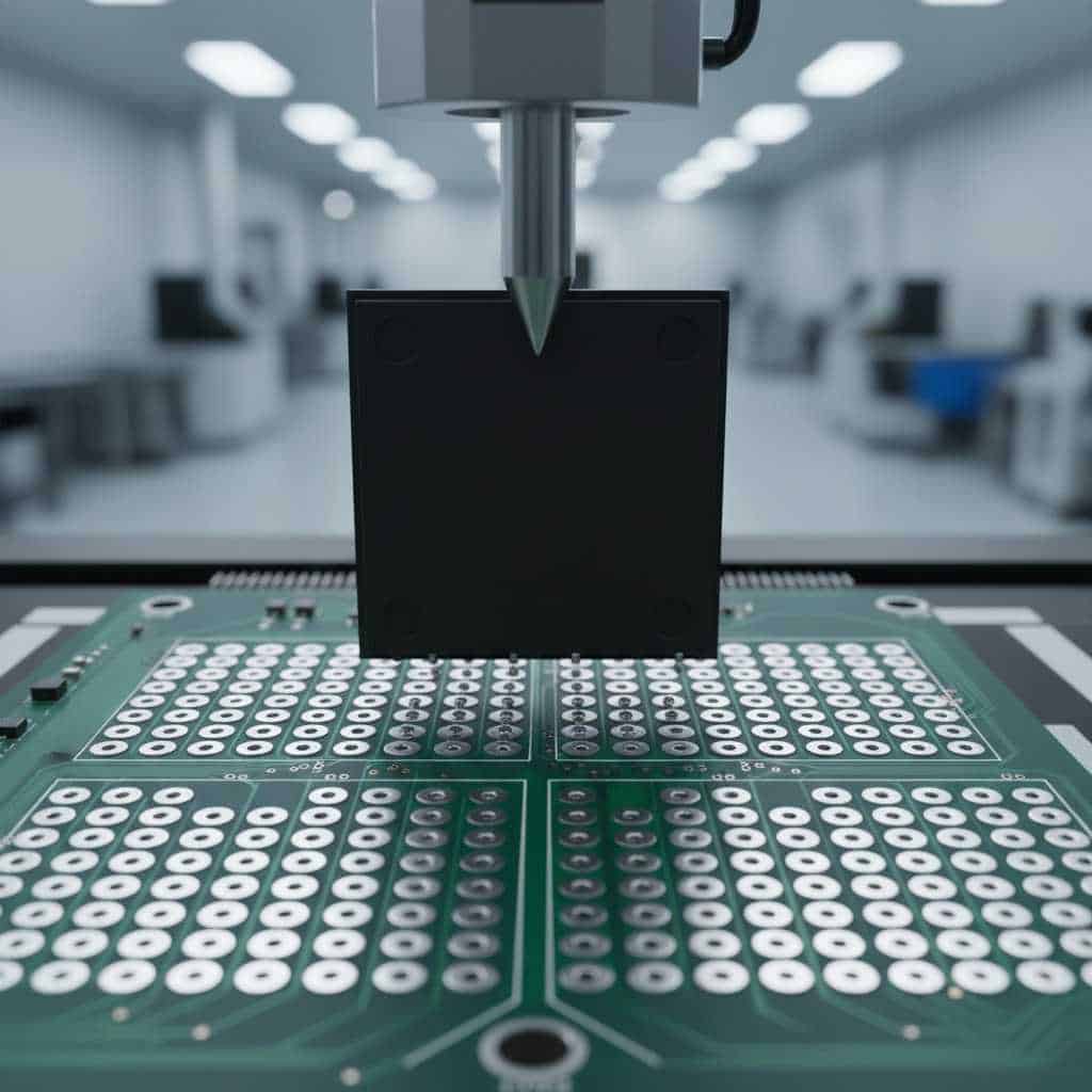
How does Bga pad selection affect the manufacturing process?
The manufacturing of a Bga pad involves tight tolerances where even microns matter. The design you choose determines how easily the board can be fabricated and how high your assembly yield will be.
Can pad design reduce assembly defects?
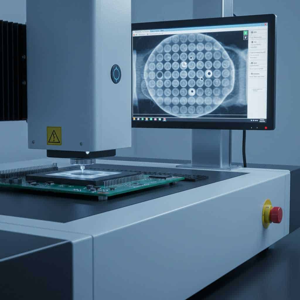
Indeed, the right design minimizes the risk of solder bridging and “insufficient solder” calls from the AOI machine. NSMD pads, for instance, offer more room for the solder to flow, reducing the chance of shorts between adjacent balls.
- Improved solder paste release from stencils.
- Reduced risk of solder ball bridging.
- Easier X-Ray Inspection of the reflowed joints.
Think about it this way: a design that is easy to build is a design that is cheaper to produce.
Key Takeaway
Consulting with your assembly partner early allows you to align your pad design with their specific SMT process capabilities for maximum yield.
| Process Factor | SMD Performance | NSMD Performance |
| Etch Tolerance | Less Critical | Critical |
| Mask Alignment | Critical | Less Critical |
| Solder Bridging | Higher Risk | Lower Risk |
Selecting a design that fits the factory’s strengths will directly lower your scrap rate.
What are the routing considerations for different Bga pads?
Routing traces out of a Bga pad array is a game of Tetris where space is the ultimate currency. NSMD pads generally provide more “real estate” between copper lands for signal escape.
Is NSMD better for high-density interconnects?
Absolutely, because the copper pad is smaller than the mask opening, you gain precious micrometers of space between pads. This allows you to route traces without violating minimum clearance rules or requiring expensive micro-vias.
- Allows for wider traces between pads.
- Reduces the number of required signal layers.
- Optimizes impedance control for high-frequency signals.
You see, it’s not just about the joint; it’s about the whole board’s architecture.
Key Takeaway
For designs requiring IPC Class 3 PCB Assembly, NSMD pads often provide the necessary clearance to meet stringent spacing requirements.
| Routing Factor | SMD Impact | NSMD Impact |
| Trace Width | Restricted | Flexible |
| Clearance | Tight | Generous |
| Layer Count | May increase | Can be minimized |
Efficiency in routing leads to a cleaner signal and a more cost-effective PCB stack-up.
When should you use a mixed Bga pad strategy?
In complex designs, you don’t always have to choose just one; a mixed strategy for the Bga pad layout can offer the best of both worlds. This involves using different pad types for different parts of the same BGA component.
Can you combine SMD and NSMD on one footprint?
It is common to use SMD pads for the corner balls of a BGA—which experience the most mechanical stress—while using NSMD for the interior signal balls. This hybrid approach reinforces the component’s structural weak points while maintaining high-speed signal integrity.
- Corners: SMD for mechanical reinforcement.
- Center: NSMD for routing and thermal life.
- Optimized for both drop tests and thermal cycling.
Believe it or not, this “best of both worlds” approach is becoming a staple in aerospace and automotive electronics.
Key Takeaway
A hybrid pad strategy allows you to engineer targeted reliability where the component needs it most without sacrificing overall performance.
[Image showing a BGA footprint with SMD corner pads and NSMD interior pads]
| Location on BGA | Suggested Pad Type | Reason |
| Outer Corners | SMD | Resists mechanical shock |
| Inner Signals | NSMD | Better routing/High speed |
| Power/Ground | Mixed | Balances current/heat |
Smart engineers use the hybrid method to solve specific failure modes identified during DFM analysis.
How does thermal management change with Bga pad types?
Thermal dissipation through a Bga pad is a major factor in the longevity of high-power processors and FPGAs. The interface between the pad and the internal planes dictates how cool the chip stays.
Does NSMD help with heat dissipation?
While the copper area is smaller, the ability to connect NSMD pads to larger copper pours on the surface can sometimes assist in lateral heat spreading. However, SMD pads provide a more direct thermal path to the PCB laminate due to their larger copper footprint.
- Influences the rate of thermal expansion (CTE).
- Affects the temperature of the solder joint during operation.
- Impacts the efficiency of thermal vias.
Are you worried about overheating? The pad design is your first line of defense.
Key Takeaway
Coordinate your pad design with your thermal via strategy to ensure that heat is efficiently moved away from the BGA package.
| Thermal Factor | SMD | NSMD |
| Heat Spreading | Moderate | High (if connected to pours) |
| Thermal Stress | High | Low |
| CTE Mismatch | More Rigid | More Compliant |
Managing heat at the pad level prevents the delamination issues that plague high-power electronics.
What are the rework challenges for each Bga pad?
Reworking a Bga pad requires removing the old component and cleaning the pads without damaging the delicate copper or mask. This is where your design choices either help or haunt the repair technician.
Is it easier to clean NSMD or SMD pads?
NSMD pads are generally easier to clean with a soldering iron and wick because there is no mask “trough” for the solder to hide in. With SMD, solder can get trapped at the mask edge, making it difficult to achieve a perfectly flat surface for the new component.
- Risk of mask “scuffing” during cleaning.
- Ease of removing residual solder.
- Survival rate of pads during multiple rework cycles.
Let’s face it, nobody wants to scrap an expensive board just because a pad lifted during a simple repair.
Key Takeaway
Choose NSMD if your product is likely to require field repairs or upgrades, as it stands up better to the manual cleaning process.
| Rework Factor | SMD Challenge | NSMD Challenge |
| Pad Lifting | Lower Risk | Higher Risk |
| Cleaning Ease | Difficult | Easy |
| Flatness | Harder to achieve | Easier to achieve |
Reliable rework starts with a pad design that can survive the heat of a rework station.
How to choose the right Bga pad for your next project?
Selecting the perfect Bga pad isn’t about following a single rule; it’s about balancing the specific trade-offs of your application. You must weigh mechanical ruggedness against signal precision.
What is the final checklist for pad selection?
Start by looking at your component’s pitch and the environment where it will live. If it’s a tiny 0.4mm pitch BGA for a smartphone, NSMD is almost mandatory; if it’s a large BGA for a vibrating industrial machine, SMD might be the winner.
- Check the component manufacturer’s datasheet recommendations.
- Evaluate the mechanical environment (shock vs. thermal).
- Assess routing density and available PCB layers.
Still unsure? Don’t worry, that’s what a professional Turnkey PCB Assembly partner is for.
Key Takeaway
Always validate your pad design through a DFM (Design for Manufacturing) check with your assembler to catch potential issues before the first board is etched.
| Application | Recommended Pad Type |
| Mobile/High-Speed | NSMD |
| Automotive/Aerospace | Hybrid (SMD Corners) |
| Industrial/Heavy | SMD |
Making the right choice today prevents the headaches of field failures tomorrow.
Conclusion
Choosing between SMD and NSMD for your BGA layout is a pivotal decision that impacts everything from signal integrity to long-term field reliability. Throughout this guide, we have explored how SMD provides the mechanical strength needed for rugged environments, while NSMD offers the precision and fatigue resistance required for high-density, high-speed modern electronics. By understanding these trade-offs, you can design boards that not only perform better but are also easier to manufacture and repair.
At Queen EMS, we specialize in navigating these complex design choices to deliver high-quality, reliable assemblies for our global partners. Whether you are dealing with tight-pitch BGAs or high-power industrial boards, we are here to help. Contact us today to discuss your next project and ensure your BGA designs are optimized for success. We are committed to powering the future of electronics through precision and partnership.
FAQ
Can I use NSMD for all my BGA designs?
Most of the time, yes. NSMD is the industry standard for most consumer and high-speed electronics because of its superior thermal fatigue resistance and routing advantages. However, if your board will be subject to extreme physical drops or vibration, you should consider SMD or a hybrid approach.
What is the best pad size for a 0.5mm pitch BGA?
Generally, a copper pad size of 0.25mm to 0.27mm is recommended for 0.5mm pitch. For NSMD, you would ensure the solder mask opening is approximately 0.1mm larger than the copper pad to provide adequate clearance.
How do I know if my assembler prefers SMD or NSMD?
You should ask them directly! Most modern assemblers prefer NSMD for its higher yield in tight-pitch applications, but they will have specific “Design for Manufacturing” (DFM) guidelines that match their equipment’s accuracy.
Can I switch from SMD to NSMD without changing the stencil?
It is not recommended. Because the solderable surface area changes between SMD and NSMD, the solder paste volume needs to be recalculated to ensure a proper joint shape and to avoid defects like “head-in-pillow.”
Does pad design affect the cost of the PCB?
Indirectly, yes. While the design itself doesn’t cost more, using NSMD can sometimes allow for fewer PCB layers due to better routing clearance, which significantly reduces the overall fabrication cost.