
Precision SMT Stencils — Engineered as Part of Our PCB Assembly Process
Custom laser-cut solder paste stencils manufactured in-house as an integrated step of our turnkey PCBA workflow. Same factory, same process, zero coordination gaps.
5 Costly Mistakes When Ordering SMT Stencils Separately
Unsynchronized Design
Separate stencil vendors and assembly plants create mismatches between aperture designs and actual PCB pads. Our integrated approach ensures perfect alignment, eliminating costly rework.
Uniform Thickness Trap
Using a single thickness causes insufficient paste on BGAs and excess paste for large components. We customize thickness strategies to guarantee flawless solder volumes everywhere.
No SPI Validation
Blind printing leaves defects undetected until after the reflow process. We utilize 3D Solder Paste Inspection to catch and correct volume deviations instantly.
Separated Lead Times
Waiting for outsourced stencils to arrive forces your assembly line to idle. Our synchronized manufacturing means assembly starts the exact moment PCBs are ready.
Poor Aperture Accuracy
Cheap stencils trigger paste bridging on fine-pitch components. We apply ±0.003mm precision cutting to ensure crisp paste release and safeguard high-density designs.
Eliminate these risks — our in-house stencil + assembly workflow solves all five.
Talk to Our EngineersHow Our SMT Stencil Service Works Differently
Purchasing stencils separately and hoping they match the assembly plant's specifications.
The stencil is engineered as the critical first step of our assembly line. Seamless in-house integration ensures perfect paste application, saving you coordination headaches.
Waiting 3-5 days for a replacement stencil when initial printing tests fail on the line.
If 3D SPI detects an issue, we laser-cut a modified stencil within 12 hours and resume production on the exact same day, keeping your delivery schedule strictly on track.
Paying an extra $125-$550 hidden cost for stencil tooling fees and separate shipping.
Stencil manufacturing is a fully integrated part of our turnkey PCBA flow. This transparent, all-inclusive workflow simplifies procurement and reduces overall assembly expenses.
Experience a smoother, risk-free assembly process.
Get an Integrated PCBA QuoteTypes of SMT Stencils We Manufacture
Framed Stencils
Mounted permanently to a rigid aluminum frame. Maintains consistent foil tension across automated SMT machines, delivering exceptional repeatability for high-volume production.
Frameless Foils
Standalone foils designed for reusable tensioning systems. Drastically cuts down on material usage and shipping dimensions, making it highly economical for rapid prototypes.
Step Stencils
Engineered with multiple thickness levels on a single foil. Delivers precise paste volumes to different areas, enabling flawless mixed-technology assembly without defects.
Nano-Coated
Treated with an advanced hydrophobic surface coating. Prevents paste from sticking to aperture walls, guaranteeing perfect transfer for your most demanding micro-BGA layouts.
Unsure which type you need for your design?
Consult Our Stencil ExpertsLaser Cut vs. Etching vs. Electroforming
| Process Type | Precision | Fine-Pitch Capability | Paste Release Performance | Cost Efficiency | Best Applied For |
|---|---|---|---|---|---|
| Laser Cut (Standard) | ±0.003mm | Excellent (Down to 0.4mm) | Very Good (Trapezoidal walls) | Highly Economical | 95% of standard to complex PCBA |
| Chemical Etching | ±0.030mm | Poor (Prone to bridging) | Fair (Hourglass-shaped walls) | Lowest (Volume only) | Low-density, basic through-hole |
| Electroforming | ±0.001mm | Superior (Below 0.3mm) | Outstanding (Smooth walls) | Premium Investment | Wafer-level, ultra-micro components |
95% of PCB assembly projects utilize laser-cut stencils — this is our standard procedure. For ultra-fine-pitch designs below 12 mil, our engineers will recommend electropolishing or nano-coating during the DFM review to ensure flawless assembly.
Get expert manufacturing recommendations for your design.
Request Free DFM ReviewSMT Stencils for Every Assembly Challenge
Fine-Pitch BGA & µBGA
Utilizing ±0.003mm laser precision, we ensure exact paste volume deposition on microscopic pads, eliminating solder bridging and maximizing your first-pass yield for complex ICs.
QFN & Leadless Packages
Custom window-pane aperture designs prevent center-pad floating and flux voiding, securing robust electrical and thermal connections for power-critical leadless components.
Mixed Technology (SMT+THT)
Step stencils with varying local thicknesses deliver optimal paste to both fine-pitch SMDs and large connectors simultaneously, preventing weak joints and manual rework.
High-Density HDI PCB
Smooth electropolished aperture walls provide superior paste release at ultra-fine pitches, securing highly reliable joints even on the most densely populated circuit boards.
Prototype & Quick-Turn
In-house frameless foil cutting syncs perfectly with your prototype fabrication schedule, accelerating your time-to-market without unnecessary tooling delays or setup overhead.
Medical & Automotive Grade
Rigorous 3D SPI validation and full process traceability guarantee consistent paste volumes board after board, ensuring life-critical reliability for high-stakes applications.
See how we handle your specific board type.
Discuss Your ApplicationSMT Stencil Manufacturing Capabilities
304 Stainless Steel (FG/SFG)
High-Precision Laser Cut
0.08mm - 0.20mm (Step Available)
±0.003mm
0.08mm (3 mil)
736mm x 736mm
0.3mm
Electropolishing / Nano-Coating
12 Hours (Integrated Workflow)
Why Our Stencils Deliver Better First-Pass Yield
In-House Manufacturing = Zero Alignment Risk
Producing stencils directly on our assembly floor ensures perfect pad alignment with your fabricated PCBs, completely eliminating the rework delays caused by outsourced mismatches.
Step Stencil for Mixed Components — Standard Service
We apply multi-level thicknesses where your design demands it, without treating it as an upsell, guaranteeing perfect solder joints for varying component sizes simultaneously.
Nano-Coating for Sub-0.5 Area Ratio Prints
Applying hydrophobic surface treatments guarantees clean paste release for demanding micro-apertures, drastically reducing cleaning frequency and printing defect rates.
12-Hour Stencil Build Time
Rapid in-house laser cutting means your stencil is ready before the bare boards even finish routing, ensuring your assembly line never sits idle waiting for tools.
SPI Closed-Loop Quality Feedback
Real-time paste inspection data is fed directly back to the automated printer, allowing instant parameter adjustments to maintain a flawless production yield.
Stencil Built Into Your Assembly Line
We engineer the stencil as a fundamental, integrated step of the PCBA process, removing hidden tooling fees and drastically simplifying your procurement chain.
Verify our capabilities against your Gerber files.
Request Engineering ReviewFrom Gerber File to First Print: Our Integrated Process
Paste Layer Extraction & Review
We extract and analyze your Gerber paste layers, identifying potential area ratio issues before manufacturing begins to guarantee precise printability.
Aperture Design Optimization
Our engineers modify aperture shapes and sizes to prevent common defects like tombstoning and solder balling, optimizing your specific layout.
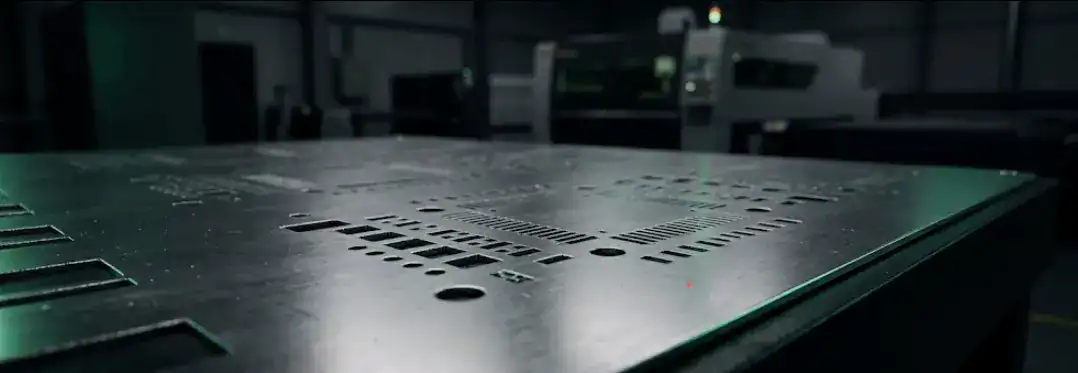
Laser Cutting on 304 Steel
High-precision laser equipment cuts the stainless steel foil, creating crisp, trapezoidal walls that ensure excellent paste release on the pads.
Electropolishing / Nano-Coating
For ultra-fine pitches, we apply advanced surface treatments to smooth out microscopic burrs, guaranteeing perfect paste transfer for micro-components.
Printing & 3D SPI Validation
The stencil goes straight to our automated printer, where 3D SPI validates the exact paste volume, ensuring flawless assembly from board one.
Experience a seamless assembly workflow.
Start Your ProjectHow We Verify Every Stencil Before Production
Aperture-to-Gerber Verification
We optically verify every cut aperture against your original Gerber files, preventing physical layout discrepancies and ensuring 100% design fidelity.
Solder Paste Inspection (SPI)
Advanced 3D scanning measures paste volume, height, and alignment on every pad, catching microscopic printing deviations before components are even placed.
Closed-Loop Adjustment
SPI data continuously communicates with our automated printers, instantly auto-correcting blade pressure and speed to maintain absolute printing consistency.
AOI + X-ray Post-Reflow
Final optical and X-ray inspections definitively confirm that our optimized paste printing has resulted in perfect, void-free solder joints across the entire board.
Ensure zero-defect assembly for your boards.
View Quality CertificationsIPC-7525 Compliant Stencil Design
Area & Aspect Ratios
Our engineers rigorously calculate the Area Ratio (>0.66) and Aspect Ratio (>1.5) for every aperture. This strict IPC compliance ensures solder paste releases cleanly from the stencil walls, preventing starved joints on your smallest components.
Aperture Modification
We proactively apply 'Home-Plate' or 'Inverted-Triangle' aperture shapes to your chip components (0402, 0201). This strategic reduction of paste volume at the edges eliminates the surface tension imbalance that causes tombstoning during reflow.
Fiducial Mark Precision
We generate perfectly matched half-etched or fully-cut fiducial marks based on your PCB panelization. This guarantees rapid, 100% accurate visual recognition by the automated SMT printer, enabling ultra-precise paste deposition.
Want to learn more about our design standards?
Download Full Design GuidelinesStandard Thickness by Component Pitch
0.05 - 0.08 mm
(2 - 3 mil)Prevents bridging on ultra-fine pitches below 0.3mm. Nano-coating highly recommended.
0.08 - 0.10 mm
(3 - 4 mil)The industry standard for modern smartphones and high-density consumer electronics.
0.10 - 0.12 mm
(4 - 5 mil)Provides the optimal balance of paste volume and release for 90% of standard PCBA projects.
0.15 - 0.20 mm
(6 - 8 mil)Ensures sufficient solder volume for robust mechanical joints on connectors and power modules.
Not sure which thickness? Upload your Gerber — our engineers will optimize the stencil design as part of your DFM review.
Upload Gerber NowStandard Frame Dimensions
| Outer Frame Size (mm) | Max Valid Print Area (mm) | Typical Application / Equipment |
|---|---|---|
| 370 × 470 | 190 × 290 | Small prototypes, manual printing, desktop SMT |
| 420 × 520 | 240 × 340 | Medium batch, standard semi-auto printers |
| 584 × 584 (23"×23") | 400 × 400 | High-volume standard, DEK / MPM compatible |
| 736 × 736 (29"×29") | 550 × 550 | Large panel arrays, server boards, LED panels |
Frequently Asked Questions
Do I need to order a stencil separately if I use your PCBA service?
No. Stencil engineering and manufacturing are completely integrated into our PCBA workflow. You do not need to place a separate order, coordinate shipping, or worry about alignment mismatches—we handle it all in-house.
When do you recommend using a Step Stencil?
Step stencils are necessary when your board contains a mix of extremely fine-pitch components (like 01005s or µBGAs requiring 0.08mm thickness) alongside large connectors (requiring 0.15mm thickness). Our engineers will identify this need during DFM.
What is Nano-Coating and is it worth it?
Nano-coating applies a hydrophobic layer to the stencil, preventing paste from adhering to the aperture walls. It is highly recommended for ultra-fine pitch components (pitch < 0.4mm) as it significantly reduces bridging and lowers wiping frequency during production.
How do you ensure the stencil perfectly matches my PCB?
Because we manufacture the bare PCB, cut the stencil, and perform the assembly in the same facility, we use the exact same Gerber dataset across all machines. Additionally, our 3D SPI (Solder Paste Inspection) verifies every print layout before components are placed.
Certified Manufacturing Excellence
Get Your PCBA Quote — Stencil Engineering Included
Upload your Gerber and BOM files. Our engineering team will review your paste layer design, recommend the optimal stencil configuration, and provide a turnkey assembly quote within 24 hours.
- Strict Non-Disclosure Agreement (NDA)
- Free DFM & Paste Layer Review
- Rapid 24-Hour Quote Processing