
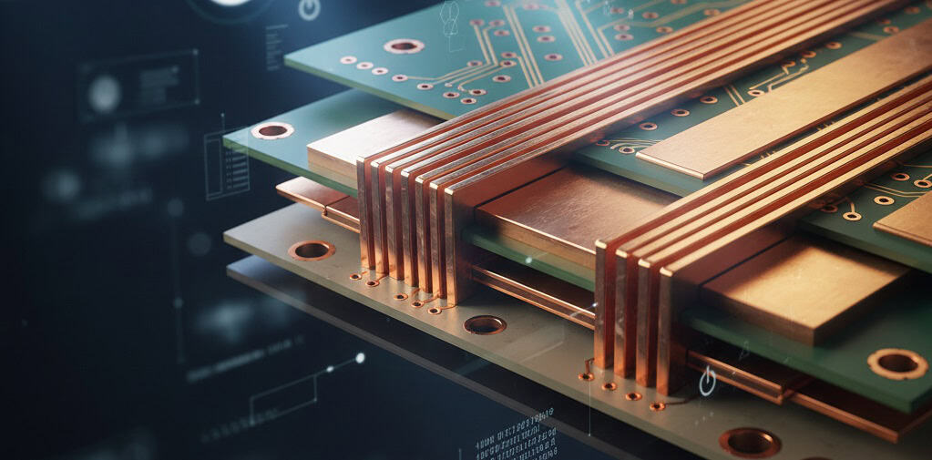
Heavy Copper PCB Manufacturing for High-Power Applications
Precision Thick Copper Fabrication · Stable Electroplating · Engineering-Driven Process
When Standard PCBs Cannot Handle High Current Loads
Your circuit board is not just carrying signals — it is the core infrastructure that supports real power delivery. As current loads increase and thermal demands grow, standard 1oz or 2oz copper simply cannot maintain the reliability your system requires. Heavy copper PCBs are engineered to solve exactly this challenge.
Rising Current Demands
Modern power electronics push higher current through tighter spaces. Standard copper weights create bottlenecks, leading to voltage drops and reduced efficiency. Heavy copper PCBs carry significantly more current per trace, enabling compact and efficient power distribution across your entire board.
Uncontrolled Temperature Rise
Thin copper layers generate excessive heat under heavy loads, causing thermal runaway that damages components and shortens product lifespan. Thick copper PCBs dissipate heat more effectively, maintaining safe operating temperatures even during sustained high-current operation.
Long-Term Reliability at Risk
Repeated thermal cycling on under-spec copper creates microcracks, delamination, and eventual trace failure. High current PCBs with proper copper weight withstand thousands of thermal cycles without degradation, delivering the long-term reliability that industrial and power applications demand.
Ensure your power electronics perform reliably from day one.
Common Problems in Heavy Copper PCB Manufacturing
Heavy copper PCB manufacturing is fundamentally different from standard board fabrication. The increased copper thickness introduces process challenges that many factories are not equipped to handle consistently. Understanding these issues helps you select a manufacturer who can deliver true quality.
Uneven Copper Plating Distribution
Electroplating thick copper layers requires precise current density control across the entire panel. Without advanced plating equipment and optimized parameters, copper thickness varies significantly between board center and edges, resulting in inconsistent electrical performance and potential failure points in high current PCB designs.
Inner Layer Lamination Deformation
Thick copper inner layers create substantial stress during the lamination process. Uncontrolled resin flow and uneven pressure distribution cause layer shifting, wrinkles, and voids. These defects compromise structural integrity and create reliability risks in heavy copper multilayer PCB stacks that only appear after thermal stress testing.
Through-Hole Copper Reliability
Plating copper inside vias on thick copper boards demands extended plating cycles. Insufficient hole wall copper leads to barrel cracking under thermal cycling, severing the connection between layers. For power electronics PCB applications, this failure mode is catastrophic and often undetectable through visual inspection alone.
Finished Board Warpage
Asymmetric copper distribution across layers generates internal mechanical stress that bows the finished board. Warped heavy copper PCBs create assembly difficulties, reduce solder joint reliability, and can cause field failures in vibration-sensitive industrial environments. Proper stack-up design and process control are essential to prevent this issue.
Avoid these manufacturing pitfalls — work with specialists who understand thick copper fabrication.
Discuss Your Heavy Copper ProjectWhy Many PCB Factories Struggle with Thick Copper Boards
Not every PCB manufacturer can produce heavy copper boards reliably. Thick copper PCB fabrication demands specialized equipment, deep process knowledge, and strict quality controls that go far beyond standard multilayer board production. Here is why most factories fall short when it matters most.
Insufficient Equipment Capability
Standard plating lines are designed for 1-2oz copper. Achieving uniform 6oz, 8oz, or 10oz copper thickness requires high-current plating systems with advanced anode configurations and real-time thickness monitoring. Factories lacking this equipment produce boards with unpredictable copper distribution and compromised current-carrying capacity.
Unstable Electroplating Control
Thick copper plating is a time-intensive process where chemical bath composition, temperature, and agitation must remain within tight tolerances for hours. Minor deviations accumulate into major defects. Factories without dedicated heavy copper process engineers frequently experience batch-to-batch variation that undermines product consistency.
Multilayer Lamination Complexity
Heavy copper multilayer PCBs require specialized prepreg selection, customized press programs, and precise resin fill calculations. Standard lamination recipes cannot accommodate the thermal mass and stress generated by thick copper layers. Without dedicated process development, delamination and registration errors become systemic issues across production runs.
Partner with a manufacturer built for thick copper fabrication challenges.
Learn About Our CapabilitiesWhat Defines a True Heavy Copper PCB
Not all thick copper boards qualify as true heavy copper PCBs. Industry standards define heavy copper as any board with copper weight of 3oz/ft² or greater. Understanding the technical distinctions helps you specify the right product for your high-power application and evaluate manufacturer capability accurately.
Copper Weight Classification
Heavy copper PCBs start at 3oz/ft² (105μm) and extend to 10oz/ft² (350μm) or beyond. Each copper weight level serves different current capacity requirements. Selecting the right copper weight balances your electrical performance needs with manufacturing feasibility and cost, ensuring optimal results for power electronics applications.
Inner vs. Outer Layer Differences
Inner and outer copper layers behave differently in manufacturing. Outer layers benefit from additive plating, while inner layers rely on subtractive etching from base copper foil. This fundamental difference affects minimum trace widths, spacing rules, and impedance control across the board stack-up in heavy copper multilayer PCB designs.
Complex Multilayer Structures
True heavy copper boards often combine thick power layers with standard signal layers in a single stack-up. This hybrid approach delivers high current capacity where needed without increasing overall board thickness unnecessarily. Achieving this requires precise material selection and controlled lamination processes tailored for mixed copper weight configurations.
Need help specifying the right copper weight for your design? Our engineers are ready.
Consult Our Engineering TeamElectroplating Control & Copper Uniformity
Achieving consistent copper thickness across every square inch of a heavy copper PCB is the single most critical factor in manufacturing quality. Our advanced heavy copper plating process combines precision current density management with real-time monitoring to deliver the uniformity your high-power designs demand.
Our Plating Control Protocol
- 1
Current Density Optimization
Each panel receives a customized current density profile based on copper weight target, board size, and pattern distribution — preventing thin spots and over-plating.
- 2
Bath Chemistry Monitoring
Plating solution composition is analyzed and adjusted at regular intervals throughout extended plating cycles, maintaining consistent deposition rates from start to finish.
- 3
Thickness Verification
Multi-point copper thickness measurements are taken on every production panel using X-ray fluorescence, ensuring each board meets the specified copper weight tolerance.
- 4
Microcrack Prevention
Controlled plating stress management and post-plating thermal treatment minimize internal stress in thick copper deposits, preventing microcrack formation during thermal cycling.
Copper Thickness Uniformity ±10%
Our high-current plating lines deliver copper thickness uniformity within ±10% across the entire panel area. This level of consistency ensures predictable current-carrying capacity and thermal performance across every trace on your heavy copper PCB.
Reliable Hole Wall Copper
Extended plating cycles with optimized throwing power ensure adequate copper deposition inside through-holes and vias. Every via connection meets IPC Class 3 standards for hole wall copper thickness, providing dependable interlayer connectivity in multilayer structures.
Zero-Defect Surface Quality
Precise agitation control and filtration throughout the plating process eliminates pitting, nodules, and surface roughness. The result is a clean, smooth copper surface that ensures excellent solderability and reliable electrical contact for your power electronics applications.
Get copper uniformity you can trust — backed by data on every panel.
Request Plating Capability DetailsOur Engineering-Driven Heavy Copper PCB Process
Every heavy copper PCB project begins with engineering — not production. Our structured four-step methodology ensures that potential issues are identified and resolved before a single panel enters the fabrication line. This front-loaded approach delivers higher first-pass yields and shorter overall lead times.
Stack-Up & Copper Thickness Review
Our engineers analyze your layer stack-up to verify copper weight assignments, dielectric spacing, and overall board thickness. We identify potential lamination risks and recommend optimized configurations that balance electrical performance with manufacturing reliability.
DFM Evaluation
Comprehensive design-for-manufacturability analysis checks trace widths, spacing, via structures, and copper balance against thick copper fabrication rules. We provide actionable feedback to optimize your design for both performance and production yield before tooling begins.
Thermal Analysis Feedback
We evaluate thermal dissipation paths and identify potential hot spots based on your copper layout and current flow patterns. Our recommendations help you achieve optimal thermal management without requiring costly board redesigns or additional heat sinking components.
Controlled Fabrication
Production proceeds with process parameters specifically tailored to your board. Custom plating profiles, lamination press programs, and etching parameters are locked in based on the engineering review, ensuring consistent results from the first panel to the last.
Start your project with engineering confidence — not guesswork.
Submit Your Design for ReviewDFM Review for High Current PCB Designs
Designing for high current is not the same as designing for standard signal integrity. Our specialized DFM review process evaluates your design against thick copper fabrication constraints and high-current performance requirements, catching issues that generic design rule checks miss entirely.
Trace Width & Current Density Analysis
Every power trace is evaluated against IPC-2152 current-carrying guidelines for the specified copper weight. We verify that trace widths provide adequate current capacity with appropriate derating factors for your operating environment and ambient temperature conditions.
- Current capacity calculation per IPC-2152
- Temperature rise modeling at full load
- Trace width optimization for board density
Heat Dissipation Path Evaluation
High current zones generate concentrated heat that must be managed through the board structure. We analyze copper plane distribution, thermal via placement, and heat spreading effectiveness to ensure your board maintains safe operating temperatures under sustained load conditions.
- Thermal via array optimization
- Copper plane heat spreading analysis
- Component thermal pad integration
Via Structure & Reliability Review
Vias in heavy copper designs carry real power — not just signals. We evaluate via size, plating requirements, and current-sharing configurations to ensure interlayer connections handle the specified current without reliability degradation over the product lifetime.
- Via current capacity verification
- Aspect ratio feasibility for thick boards
- Redundant via recommendations
Etching & Registration Feasibility
Thick copper requires wider etch compensation and tighter registration control. We check that your design accommodates the etching undercut inherent in heavy copper processing, and verify that pad-to-trace clearances maintain electrical isolation after fabrication.
- Etch factor compensation analysis
- Minimum annular ring calculation
- Clearance and creepage validation
Get expert DFM feedback on your high current design — free with every quote.
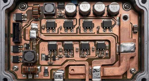
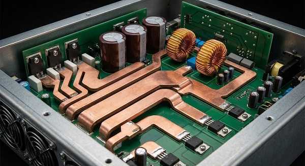
Upload Your Design FilesHeavy Copper Multilayer PCB Manufacturing Capability
Manufacturing multilayer heavy copper PCBs requires a combination of advanced equipment, controlled processes, and deep technical experience. Our production facility is purpose-built for thick copper fabrication, delivering consistent quality from prototype quantities through full production volumes.
Multilayer Thick Copper Stack-Ups
We fabricate heavy copper multilayer PCBs with up to 20+ layers, combining thick power planes with standard signal layers in a single integrated structure for complex power and control applications.
- Up to 20+ layer heavy copper construction
- Mixed copper weights: 1oz signal + 6oz power layers
- Controlled impedance on signal layers
- Blind and buried via options available
High Voltage Structure Support
Our lamination process maintains precise dielectric thickness control between heavy copper layers, providing the insulation integrity required for high-voltage power electronics applications and safety certification compliance.
- Dielectric thickness control ±10%
- Hi-pot testing per IPC standards
- UL-recognized base materials
- Creepage and clearance verification
Batch Consistency & Stability
Every production batch runs under locked process parameters with statistical process control monitoring. Consistent lamination pressure profiles, plating conditions, and etching parameters ensure identical performance from the first unit to the thousandth.
- SPC-monitored critical parameters
- Cross-section analysis per lot
- Full traceability from materials to shipment
- Cpk ≥ 1.33 on key process metrics
See how our manufacturing capability matches your project requirements.
Request Capability OverviewAdvanced Equipment for Thick Copper Fabrication
Precision heavy copper PCB manufacturing starts with the right equipment. Our production floor features dedicated thick copper processing lines with equipment specifically selected and configured for high copper weight fabrication — not repurposed from standard board production.
High-Current Plating Lines
Dedicated electroplating systems with programmable rectifiers deliver precise current density control for uniform deposition of 3oz to 10oz+ copper, with real-time thickness feedback during extended plating cycles.
Automated Alignment Systems
Optical registration equipment maintains layer-to-layer alignment accuracy within ±2mil on thick copper multilayer boards, compensating for the material movement inherent in heavy copper lamination processes.
AOI & X-Ray Inspection
Automated optical inspection and X-ray analysis verify copper integrity, via fill quality, and internal layer registration on every production panel — catching defects invisible to standard visual inspection methods.
Batch Process Control
Integrated manufacturing execution systems track every process parameter across the production cycle, enabling real-time quality monitoring and full traceability from raw material receipt through final inspection and shipment.
Tour our facility capabilities — virtually or in person.
Schedule a Factory TourUrgent & Low Volume Heavy Copper PCB Production
Heavy copper PCB projects often come with tight deadlines and small quantities — prototype validation, pre-production testing, or emergency replacement boards. Our production system is structured to handle low volume heavy copper PCB orders with the same process rigor and quality commitment as full production runs, delivered on an accelerated timeline.
Expedited Heavy Copper Fabrication
When project timelines demand speed, our dedicated express production line prioritizes your heavy copper boards without sacrificing the controlled plating and lamination processes that ensure quality.
- Accelerated engineering review within hours
- Priority scheduling on thick copper plating lines
- Same quality standards as standard lead time
Small Batch Production Support
From 1 piece to 100 pieces, our production workflow accommodates small quantities without the cost penalties or quality compromises that many heavy copper manufacturers impose on low volume orders.
- No minimum order quantity requirement
- Full process control on every batch
- Prototype to pre-production bridge support
Worldwide Express Delivery
Finished boards reach your facility through our established international logistics network. We coordinate with major express carriers to deliver heavy copper PCBs to destinations across North America, Europe, and Asia.
- DHL, FedEx, UPS express options
- Custom packaging for thick copper boards
- Real-time shipment tracking provided
Need heavy copper boards fast? Tell us your deadline — we will find a way.
Get Expedited QuoteChina-Based Heavy Copper PCB Manufacturer with Global Delivery
Choosing a heavy copper PCB supplier from China does not mean compromising on quality or communication. Our factory combines advanced manufacturing infrastructure with a transparent, export-oriented workflow built specifically for international clients who demand accountability and reliability.
Why Global Clients Choose Our Factory
Factory Direct Model
You work directly with our production facility — no trading companies, no middlemen. This factory direct approach gives you complete visibility into manufacturing progress, direct access to process engineers, and pricing that reflects actual production costs without broker markups.
Transparent Production Process
Every order includes documented production milestones with photographic evidence at critical process stages. You receive real-time status updates, inspection reports, and test data throughout the manufacturing cycle — no surprises, no guesswork about where your boards stand.
Proven Export Experience
Years of serving clients across North America, Europe, and Asia have shaped our processes for international business. English-speaking engineers, export-compliant documentation, and established logistics partnerships ensure smooth collaboration regardless of where you are located.
Experience the factory direct advantage — quality, transparency, and competitive pricing.
Connect with Our TeamStable Batch Control for Industrial & Power Applications
Industrial heavy copper PCB applications demand more than just meeting spec on a single board — they require repeatable quality across every unit in every batch, over months and years of production. Our process control infrastructure delivers the consistency that industrial and power electronics customers depend on for long-term product reliability.
Quality Consistency Metrics
Statistical Process Control
Critical parameters including copper thickness, dielectric spacing, and hole wall quality are monitored with SPC charts. Process drift is detected and corrected before it affects product quality.
Cross-Section Analysis Per Lot
Every production lot includes destructive cross-section samples to verify internal layer structure, copper thickness, and via integrity. Results are documented and available for customer review.
Full Material Traceability
From copper foil lot numbers to laminate batch codes, every material entering your board is traceable. In the event of a field issue, we can identify the exact materials and process conditions used.
Locked Process Parameters
Once your board passes first article validation, all process parameters are locked in our manufacturing execution system. Subsequent batches run under identical conditions, ensuring unit-to-unit consistency.
Long-Term Production Stability
Locked process recipes and controlled material sourcing ensure your heavy copper PCBs perform identically whether you order today or twelve months from now. This consistency eliminates the variability that plagues customers who switch between suppliers or work with factories lacking formal process control.
Comprehensive Quality Documentation
Every shipment includes complete inspection reports, test data, and compliance certificates. For customers requiring IPC Class 3 or application-specific testing, we provide the documentation package your quality team needs for incoming inspection and traceability records.
Strict Quality Gate System
Multiple inspection checkpoints throughout the manufacturing process catch defects at the earliest possible stage. Boards must pass each quality gate before advancing, ensuring only fully conforming product reaches final inspection and shipment to your facility.
Require consistent, documented quality for your industrial application? Let's talk.
Request Quality Data SamplesApplications Suitable for Heavy Copper PCBs
Heavy copper PCBs serve as the backbone of systems where high current, thermal management, and long-term reliability are non-negotiable. Our power electronics PCB manufacturing capability supports the most demanding applications across multiple industries.
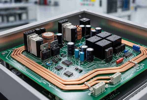
Industrial Control Systems
Motor drives, PLCs, and factory automation controllers rely on heavy copper PCBs to handle high current switching loads while maintaining precise signal integrity for control circuitry within the same board structure.
- Motor drive power stages
- PLC power distribution boards
- Industrial inverter modules
Power Supplies & Converters
AC/DC power supplies, DC/DC converters, and voltage regulators require thick copper traces to efficiently handle high current paths while managing the substantial heat generated during power conversion processes.
- Switch-mode power supplies
- DC/DC converter modules
- High-efficiency rectifier boards
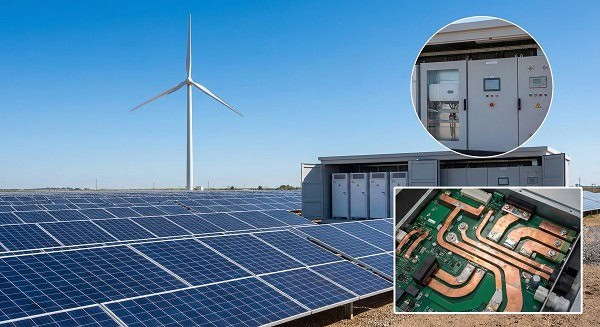
Renewable Energy Systems
Solar inverters, wind turbine controllers, and battery management systems operate under sustained high current loads in challenging thermal environments. Heavy copper construction ensures reliable performance over decades of continuous operation.
- Solar string inverter boards
- Wind turbine power converters
- Battery management systems
Automotive Power Modules
EV power inverters, onboard chargers, and DC-DC converters demand heavy copper PCBs that withstand extreme thermal cycling and vibration while maintaining high current capacity in compact form factors required by automotive packaging constraints.
- EV traction inverter boards
- Onboard charger power stages
- Automotive DC-DC converters
Inverters & UPS Systems
Grid-tied inverters and uninterruptible power supplies handle critical power conversion under continuous load. Heavy copper PCBs provide the current capacity and thermal stability needed for 24/7 operation in mission-critical power infrastructure applications.
- Grid-tied inverter power stages
- UPS rectifier and inverter boards
- Frequency converter modules
Your application requires heavy copper — let our engineers help optimize your board design.
Discuss Your ApplicationRequest a Heavy Copper PCB Quote
If your design requires high copper weight, high current capacity, stable multilayer structure, and reliable thermal performance — our engineering team is ready to review your project and deliver a detailed quotation with DFM feedback.
Trusted by power electronics, industrial automation, and renewable energy companies worldwide. Your designs are protected by strict NDA and confidentiality protocols. Engineering review and DFM feedback included with every quotation at no additional cost.