
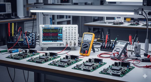
PCBA testing is the essential process of validating the functionality, connectivity, and structural integrity of a populated circuit board to ensure every component performs correctly under operational stress. Imagine shipping ten thousand units of your new smart controller only to discover a 15% failure rate in the first month due to cold solder joints. For B2B manufacturers, these preventable defects lead to devastating recall costs, tarnished brand reputations, and lost contracts. Here’s the deal: without a multi-layered verification strategy, you are essentially gambling with your hardware’s reliability. By implementing rigorous PCBA testing at every production stage, you catch faults before they leave the factory floor, turning potential liabilities into high-performance assets. At Queen EMS, we treat inspection as an art form, ensuring your designs transition from the assembly line to the field with absolute zero-defect certainty.+4
1. Why is PCBA Testing the backbone of quality?

PCBA Testing serves as the definitive filter that confirms whether the complex assembly of silicon and copper meets the engineering specifications intended during the design phase. It is the only way to prove that every bridge, via, and component lead is electrically sound. You might be wondering if visual inspection alone is enough for modern high-density boards.+4
- Identifies hidden solder bridges under BGA components.+3
- Verifies component values to prevent wrong parts installation.+3
- Simulates real-world electrical stress to find early-life failures.+2
How does testing reduce long-term costs?
By catching defects early, you avoid the compounding costs of rework that occur once the board is fully enclosed in a chassis. This proactive approach is a cornerstone of professional PCBA testing where efficiency and reliability are paramount. Wait, there’s more.+4
- Early detection prevents the “scrap” of expensive final assemblies.+2
- Reliable data allows for continuous process improvement in the factory.+3
Key Takeaway: Rigorous initial testing is the most cost-effective way to manage a hardware product’s lifecycle.+2
| Testing Level | Primary Goal | Cost Impact |
| Early Stage | Component Validation | Lowers Rework Costs +3 |
| Final Stage | System Performance | Prevents Field Recalls +2 |
Analysis: Moving from human-only checks to automated testing increases defect detection rates and lowers long-term overhead.+1
2. Why is AOI essential in modern PCBA Testing?
PCBA Testing utilizes Automated Optical Inspection (AOI) to scan boards for placement and soldering defects with microscopic precision. It is the standard for high-speed production lines where human fatigue would lead to missed errors. Believe it or not, AOI can check thousands of solder joints in seconds.+4
- Detects missing, misaligned, or upside-down components.+2
- Measures solder paste volume to ensure structural integrity.+2
Is AOI enough for complex BGA chips?
While AOI is incredible for surface-level parts, it cannot “see” through components to the hidden solder balls underneath. This is why we often pair it with PCBA testing methods like X-ray for total coverage. Ready for the good part? +4
- AOI provides instant feedback to pick-and-place machines.+2
- It maintains consistent quality regardless of shift length.+3
Key Takeaway: AOI eliminates the variability of human error in high-volume assembly projects.+3
| Inspection Type | Human Eye | AOI System |
| Speed | Slow/Variable | Extremely Fast +2 |
| Repeatability | Low | 100% Consistent +3 |
Analysis: Automating visual checks ensures that manufacturing defects are caught before the board moves to more expensive electrical testing stages.+1
3. How does ICT ensure electrical PCBA Testing accuracy?
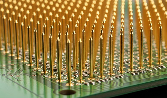
PCBA Testing through In-Circuit Testing (ICT) provides a “bed of nails” that probes individual components to verify their electrical health. It treats the board as a collection of individual parts, ensuring no resistor or capacitor was damaged during reflow. But here’s the kicker.+4
- It checks for shorts, opens, and resistance values.
- It identifies faulty ICs before they are powered up fully.
When should you invest in ICT fixtures?
ICT is ideal for high-volume B2B orders because the test time per board is incredibly short. For smaller runs, our PCBA testing capabilities often utilize flying probe technology to save on fixture costs. You might be wondering if the cost is justified.+4
- It provides 100% electrical verification of all analog parts.+1
- The diagnostic data tells you exactly which part is failing.+2
Key Takeaway: ICT is the most reliable way to guarantee that every component on the board is electrically sound.+3
| Parameter | ICT (Fixture) | Flying Probe |
| Setup Cost | High | Low +3 |
| Test Speed | Very Fast | Slow +2 |
Analysis: Selecting the right ICT method depends on balancing upfront tooling costs against long-term production volume.+1
4. Why is Functional Testing (FCT) vital for PCBA Testing?
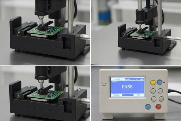
PCBA Testing is only truly complete once Functional Testing confirms the board performs its intended task in a real-world scenario. FCT simulates the final application, plugging the board into a rig that mimics its end-use. What’s the real story? +4
- It validates the interaction between hardware and firmware.+1
- It checks communication ports like Wi-Fi, Bluetooth, and USB.+3
Can FCT identify software-related failures?
Yes, because the board is powered on and running its code, FCT can catch bugs that simple electrical tests would never see. We use PCBA testing to ensure that the user experience is flawless from the first boot. It’s a game changer.+4
- It ensures the board stays within thermal limits during operation.+3
- It provides a “Pass/Fail” result based on actual performance.+3
Key Takeaway: FCT is your final guarantee that the customer receives a working, high-performance product.+2
![Photorealistic image of a custom functional test rig with a PCB under power and a digital display showing “PASS”]https://r.jina.ai/i/44053676449e4942858597e748f3b207)
| Feature | ICT Focus | FCT Focus |
| Test Level | Individual Parts | Full System +3 |
| Main Benefit | Structural Integrity | Operational Logic +3 |
Analysis: Functional testing provides the bridge between a correctly built board and a correctly functioning device.+1
5. How does X-Ray solve hidden PCBA Testing gaps?
PCBA Testing reaches a new level of depth with X-ray inspection, which allows engineers to see through opaque materials. This is crucial for BGA (Ball Grid Array) components where the solder joints are hidden directly under the chip body. This is where it gets interesting.+4
- It detects solder bridging that is invisible to cameras.+3
- It reveals “voiding” or air bubbles inside the solder joints.+2
Is X-ray necessary for all high-end boards?
If your design uses fine-pitch BGA or QFN parts, X-ray is the only way to ensure those hidden connections are solid. Professional PCBA testing protocols mandate X-ray to prevent catastrophic failures in high-vibration environments. Ready for the good part? +4
- It provides a non-destructive way to verify internal alignment.+3
- It is vital for verifying the quality of multi-layer PCB vias.+3
Key Takeaway: X-ray inspection removes the “blind spots” from your quality control process for advanced electronics.+3
| Defect Type | AOI Visibility | X-Ray Visibility |
| Surface Short | 100% | 100% +3 |
| BGA Bridge | 0% | 100% +3 |
Analysis: For modern component packaging, X-ray is the only method to guarantee structural integrity deep within the board.+1
6. What role does Flying Probe play in PCBA Testing?
PCBA Testing via Flying Probe is the most flexible electrical verification method for prototypes and low-volume batches. It uses robotic arms to move probes to specific points on the board, eliminating the need for expensive custom fixtures. Believe it or not, it can start testing just hours after the design is finalized.+4
- It is perfect for rapid R&D and engineering samples.+3
- It can test extremely dense boards with very small pads.+3
Why choose Flying Probe over ICT?
For small quantities, the high cost of an ICT fixture is often prohibitive, making the flying probe the smarter financial choice. We integrate this into our PCBA testing services to keep costs low for our clients’ innovation cycles. What’s the catch? +4
- It is slower than ICT, making it less ideal for mass production.+3
- It provides the same deep electrical diagnosis as a fixed fixture.+3
Key Takeaway: Flying probe testing offers high-precision electrical verification without the barrier of upfront tooling costs.+2
| Project Scale | Preferred Test | Advantage |
| Prototype | Flying Probe | Low Setup Cost +3 |
| Mass Production | ICT Fixture | High Throughput +2 |
Analysis: Utilizing the right equipment at each stage of development ensures technical accuracy while maintaining budget control.+1
7. How does Burn-in testing validate PCBA Testing?
PCBA Testing often includes “Burn-in” testing, which involves running the board at elevated temperatures for an extended period. This forces “infant mortality” failures—components that would have failed in the first month of use—to fail in the factory instead. But here’s the kicker.+4
- It simulates years of operational stress in just 24–48 hours.+3
- It ensures the board remains stable under extreme thermal conditions.+2
Is burn-in required for industrial products?
For B2B hardware used in oil and gas, automotive, or aerospace, burn-in is often a mandatory safety requirement. Our PCBA testing lab uses calibrated ovens to push your hardware to its limits. You might be wondering if your board can survive.+4
- It validates the longevity of the power management system.+3
- It provides peace of mind for mission-critical deployments.+3
Key Takeaway: Burn-in testing filters out the weakest units, ensuring only the most robust hardware reaches your client.+2
| Environment | Stress Method | Goal |
| High Heat | Thermal Chamber | Weed out weak ICs +3 |
| Vibration | Shaker Table | Check Solder Integrity +3 |
Analysis: High-stress simulations are the final frontier for establishing long-term product reliability in hostile environments.+1
8. Why is Traceability vital in PCBA Testing?
PCBA Testing data must be linked to a robust traceability system so that every board’s history is recorded. This allows us to track which components were used, which technician inspected them, and the exact test results for every unit. Here is the deal.+4
- It allows for targeted recalls if a specific component batch is faulty.+3
- It provides a “birth certificate” for every high-reliability assembly.+3
How does traceability protect your brand?
In the event of a field failure, traceability data allows us to determine if the issue is systemic or an isolated incident. We use professional PCBA testing to manage this data, giving you the documentation needed for regulatory compliance. The bottom line is.+4
- It tracks the origin of every silicon chip back to the supplier.+3
- It builds trust with high-tier B2B customers and auditors.+3
Key Takeaway: Total traceability turns a simple circuit board into a professional, accountable asset for your company.+2
| Tracking Level | Information Provided | Benefit |
| Batch Level | General Production Date | Basic Accountability +3 |
| Serial Level | Individual Test Logs | Complete Legal Defense +3 |
Analysis: Detailed documentation is the bridge between a simple assembly and an enterprise-ready hardware product.+1
9. How to optimize Design for PCBA Testing (DFT)?
PCBA Testing is significantly more efficient when the board is designed with testing in mind from day one. This practice, called Design for Test (DFT), involves placing dedicated test pads that probes can easily reach. You might be wondering how much space this takes.+4
- It reduces the complexity and cost of test fixtures.+3
- It allows for 100% test coverage of all critical nets.+3
What are the top DFT tips for engineers?
Keep your test pads on one side of the board to allow for single-side probing, which is much cheaper than double-sided fixtures. We often help clients refine their PCBA testing to ensure it is optimized for our automated lines. Ready for the good part? +4
- Ensure test pads are not covered by tall components.+3
- Use a consistent grid for test points to simplify the fixture.+2
Key Takeaway: Investing in DFT during the design phase will save you thousands of dollars in production and testing costs.+2
| Design Choice | Impact on Test | Cost Direction |
| Single-Side Pads | Simple Fixture | ↓ Lower Cost +3 |
| Labeled Nets | Faster Debugging | ↓ Faster Turnaround +3 |
Analysis: Early collaboration between engineering and manufacturing reduces time-to-market by streamlining the inspection phase.+1
10. How to select the right PCBA Testing partner?
PCBA Testing is only as good as the equipment and expertise of the factory performing it. You need a partner who doesn’t just “check boxes” but proactively finds ways to improve your product’s reliability. Here is the deal.+4
- Look for a partner with in-house AOI, ICT, and FCT capabilities.+3
- Ensure they provide detailed, transparent quality reports.+1
What sets a professional factory apart?
A professional factory will have an engineering team that can help you design custom functional test rigs specifically for your product. At Queen EMS, we treat PCBA testing as a core competitive advantage, ensuring your hardware is field-ready. Wait, there’s more.+4
- They should offer environmental stress testing as an option.+1
- They must be responsive to troubleshooting and failure analysis.+1
Key Takeaway: The right partner acts as an extension of your own engineering team, prioritizing your product’s success.+3
| Selection Criteria | Importance | Impact |
| Equipment Level | High | Precision and Coverage +3 |
| Expert Staff | High | Problem Solving Ability +1 |
Analysis: Partnering with a data-driven assembly house is the final step in securing a stable B2B supply chain.+1
Conclusion
In summary, we have explored how a systematic PCBA testing strategy—combining AOI, ICT, and FCT—is the only way to ensure the long-term reliability of your B2B hardware. By catching defects early, optimizing for testability, and insisting on total traceability, you protect your company from the devastating financial and reputational impact of field failures. You should know that quality is not an act; it is a habit that must be designed into every step of the assembly process. Our mission at Queen EMS is to provide the transparent, high-performance manufacturing services that your innovations deserve. If you are looking to secure your supply chain and elevate your product standards, please contact us today to discuss your testing needs. Let’s build something that stays working, together.+4
FAQ
Q1: Can I rely on AOI alone for high-reliability boards? Absolutely not. While AOI is excellent for visual defects, it cannot verify electrical performance or see internal solder voids, which is why ICT and X-ray are required for high-tier products.+1
Q2: What’s the best way to handle testing for low-volume prototypes? The best approach is to use Flying Probe testing. It provides the high-precision electrical verification of ICT without the high cost of building custom hardware fixtures for small quantities.+1
Q3: How do I know if my design has enough test points? We recommend a Design for Test (DFT) review. Generally, every electrical net should have at least one accessible test point to achieve 100% coverage during ICT.+1
Q4: Can PCBA testing identify counterfeit components? Yes, ICT and FCT are often the first to flag counterfeit parts. These components rarely meet the exact electrical specs or logic behaviors of the genuine manufacturer.+1
Q5: How long does a typical functional test take per board? It depends on complexity, but most FCT cycles take between 30 seconds to 3 minutes. We work to optimize this so it does not become a bottleneck in your production schedule.