
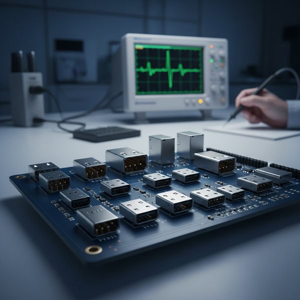
USB Pinout is a standardized map of electrical connections within a USB connector that defines how power and data are transmitted between devices. Have you ever spent hours debugging a custom PCB only to realize the USB data lines were swapped, or worse, the power pins were misaligned? For hardware engineers and procurement managers, a single wiring error in the USB Pinout can lead to fried prototypes, delayed production cycles, and significant financial loss. As a leading PCB assembly factory, we understand these technical frustrations and provide this guide to ensure your hardware designs are robust, compliant, and ready for mass production.
What is a USB Pinout?
A USB Pinout is a technical diagram that specifies the assignment of each physical pin in a USB connector to its corresponding electrical function, such as power (VBUS), ground (GND), and differential data pairs (D+ and D-). This configuration ensures that cables and devices from different manufacturers can communicate seamlessly without causing short circuits.
Why does pin accuracy matter?
When you are designing a complex PCB, maintaining signal integrity is your top priority. Incorrectly mapped data lines can introduce noise or completely disable high-speed communication.
- Preventing Damage: Ensuring VBUS and GND are never reversed.
- Signal Integrity: Maintaining impedance for high-speed data pairs.
- Compliance: Meeting USB-IF standards for global compatibility.
How do engineers use these diagrams?
You likely rely on these diagrams during the schematic capture and layout phases of your design. Accurate pin mapping is the foundation of a functional SMT assembly process.
- Schematic Entry: Linking physical pins to logical net names.
- PCB Layout: Routing traces based on pin positions.
- Testing: Using breakout boards to verify connectivity.
Key Takeaway: Understanding the foundational map of a USB Pinout is the first step in ensuring your hardware prototype transitions successfully to volume manufacturing.
| Component | Function | Importance |
| VBUS | Power Delivery | Essential for device operation |
| D+/D- | Data Transmission | Required for communication |
| GND | Ground Reference | Vital for circuit stability |
The precision of your initial design phase directly dictates the yield and reliability of the final electronic assembly.
What are the types of USB connectors?
The USB Pinout varies significantly across different connector types, ranging from the classic 4-pin Type-A to the complex 24-pin Type-C interface. Choosing the right connector depends on your project’s power requirements, data speed needs, and physical space constraints.
What characterizes the Standard-A connector?
The Type-A connector remains the most recognizable interface in the industry, typically found on host devices like PCs and hubs.
- Pin Count: Features 4 pins for USB 2.0 and 9 pins for USB 3.0.
- Durability: Designed for thousands of insertion cycles.
- Usage: Primary power and data source for peripherals.
Why choose Micro or Mini USB?
While being phased out by Type-C, these smaller connectors are still prevalent in legacy industrial equipment and compact consumer electronics.
- Space Saving: Ideal for thin-profile handheld devices.
- Mini-USB: Common in older cameras and GPS units.
- Micro-USB: Features a 5th “ID” pin for OTG (On-The-Go) functionality.
Key Takeaway: Selecting the appropriate connector type early in the design phase ensures that your USB Pinout aligns with both user expectations and manufacturing capabilities.
| Connector Type | Pin Count (2.0) | Standard Application |
| Type-A | 4 Pins | Host controllers and chargers |
| Micro-B | 5 Pins | Legacy mobile devices |
| Type-C | 24 Pins | Modern high-speed peripherals |
Proper connector selection is crucial for optimizing the THT PCB assembly process and ensuring long-term product durability.
How is the USB 2.0 Pinout configured?
The USB Pinout for the 2.0 standard is the industry baseline, utilizing a simple four-wire system to handle power and low-to-high speed data. It remains the go-to choice for cost-sensitive applications where extreme data throughput is not a requirement.
What are the four core pins?
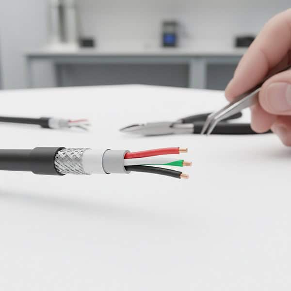
Standard USB 2.0 cables use a color-coded system that engineers must strictly follow to ensure device safety.
- Pin 1 (Red): VBUS (+5V power supply).
- Pin 2 (White): Data Minus (D-).
- Pin 3 (Green): Data Plus (D+).
- Pin 4 (Black): Ground (GND).
Is there a hidden fifth pin?
In Micro and Mini connectors, a fifth pin known as the “ID” pin is introduced to allow the device to act as either a host or a client.
- Host Mode: ID pin is shorted to Ground.
- Device Mode: ID pin is left floating (NC).
- Application: Essential for smartphones connecting to flash drives.
Key Takeaway: Mastering the 4-wire USB Pinout allows for efficient quick-turn PCB prototyping without unnecessary complexity.
| Pin # | Wire Color | Signal Name |
| 1 | Red | VCC / VBUS (+5V) |
| 2 | White | Data- (D-) |
| 3 | Green | Data+ (D+) |
| 4 | Black | Ground (GND) |
Reliable wiring at the 2.0 level prevents the vast majority of common power-related failures in the field.
What makes the USB 3.0 Pinout different?
The USB Pinout for 3.0 (now known as USB 3.2 Gen 1) adds five additional pins to the existing 2.0 architecture to support “SuperSpeed” data rates of up to 5Gbps. This backward-compatible design allows newer devices to work with older ports while offering a massive performance boost when paired correctly.
How are the extra pins used?
These additional pins form two differential pairs specifically dedicated to high-speed data transmission and reception.
- StdA_SSRX+/-: SuperSpeed receiver differential pair.
- StdA_SSTX+/-: SuperSpeed transmitter differential pair.
- GND_DRAIN: Provides a dedicated return path for high-speed signals.
Why is shielding more critical here?
At 5Gbps and higher, electromagnetic interference (EMI) becomes a major challenge for PCB designers.
- Twisted Pairs: High-speed lines must be routed as differential pairs.
- Controlled Impedance: Traces must maintain 90 ohms differential impedance.
- Crosstalk: Extra ground pins are used to isolate signals.
Key Takeaway: Designing for a 3.0 USB Pinout requires advanced mixed-technology assembly expertise to handle increased signal density.
| Signal Group | Pin Purpose | Data Rate Support |
| Legacy | Backward compatibility | Up to 480 Mbps |
| SuperSpeed TX | Outgoing high-speed data | Up to 5 Gbps+ |
| SuperSpeed RX | Incoming high-speed data | Up to 5 Gbps+ |
Integrating SuperSpeed capabilities demands a higher level of precision in both the layout and the assembly stages.
Why is the USB Type C Pinout so complex?
The USB Pinout for Type-C is a masterpiece of engineering, featuring 24 pins in a flippable, symmetrical design that supports data, power, and video. It is the most versatile interface available, but it also presents the steepest learning curve for hardware designers.
How does the symmetry work?
The 24 pins are arranged in two rows (A and B), where most signals are mirrored, allowing the cable to work regardless of which way it is inserted.
- VBUS/GND: Located at the corners and center for high current.
- Configuration Channel (CC): Pins CC1 and CC2 detect cable orientation.
- High-Speed Lanes: Four sets of TX/RX pairs for massive throughput.
Can it handle power and video?
Beyond standard data, this pinout supports Power Delivery (PD) up to 240W and Alternate Modes like DisplayPort.
- Sideband Use (SBU): Used for auxiliary signals in Alt-Mode.
- Power Negotiation: CC pins communicate power requirements.
- Versatility: Replaces HDMI, Power Jacks, and Data ports.
Key Takeaway: The USB Pinout of Type-C is the future of connectivity, requiring sophisticated BGA assembly techniques for its dense connector footprint.
| Pin Row | Key Signals | Primary Function |
| Row A | A1-A12 | Primary data/power interface |
| Row B | B1-B12 | Mirrored/Redundant interface |
| CC1/CC2 | Orientation | Logic and power negotiation |
The shift to Type-C represents a move toward a universal interface that simplifies the user experience while challenging the designer.
How to wire a Micro USB Pinout?
Wiring a USB Pinout for Micro-USB requires attention to the compact 5-pin layout, which includes the critical ID pin for OTG support. This connector is small and fragile, making the soldering and strain relief aspects of your design vital for longevity.
What is the pin sequence?
Unlike the larger Type-A, the Micro-USB pins are closely spaced, usually at a 0.65mm pitch.
- Pin 1: +5V (VBUS).
- Pin 2: Data- (D-).
- Pin 3: Data+ (D+).
- Pin 4: ID (OTG Identifier).
- Pin 5: Ground (GND).
How do you handle the ID pin?
For most standard charging or data cables, the ID pin is left unconnected, but for host cables, it must be grounded.
- Charging Cable: ID pin is NC (Not Connected).
- OTG Cable: ID pin is shorted to GND at the Micro-B end.
- Design Tip: Use a 0-ohm resistor on your PCB to switch between modes easily.
Key Takeaway: Precise wiring of the Micro USB Pinout is essential for devices used in industrial automation where reliability is paramount.
| Pin Number | Signal | Wire Color (Standard) |
| 1 | VBUS | Red |
| 4 | ID | Usually NC or Ground |
| 5 | GND | Black |
Small-scale connectors like Micro-USB require specialized assembly tools to ensure high-quality solder joints.
What are the Power Delivery (PD) Pinout requirements?
Integrating Power Delivery into your USB Pinout design allows your device to negotiate high voltage and current, reaching up to 48V at 5A. This is not possible with standard legacy wiring and requires a dedicated PD controller chip.
Which pins handle the power?
While VBUS and GND carry the actual current, the CC pins are the “brains” behind the power negotiation.
- VBUS: Thicker traces or multiple layers are needed for high current.
- CC1/CC2: These pins “talk” to the charger to ask for more voltage.
- GND: A solid ground plane is essential to prevent voltage drops.
How do you protect your circuit?
With high power comes high risk; protection components must be integrated into your pinout design.
- TVS Diodes: To protect against Electrostatic Discharge (ESD).
- OVP/OCP: Over-voltage and over-current protection circuits.
- Thermal Management: Heat sinks or copper pours near power pins.
Key Takeaway: A robust USB Pinout for Power Delivery is critical for high-performance hardware like robotics and drones.
| PD Level | Max Voltage | Max Current |
| Standard | 5V | 3A |
| PD 2.0/3.0 | 20V | 5A |
| EPR (PD 3.1) | 48V | 5A |
Designing for high-wattage power delivery requires a deep understanding of both electrical safety and thermal dynamics.
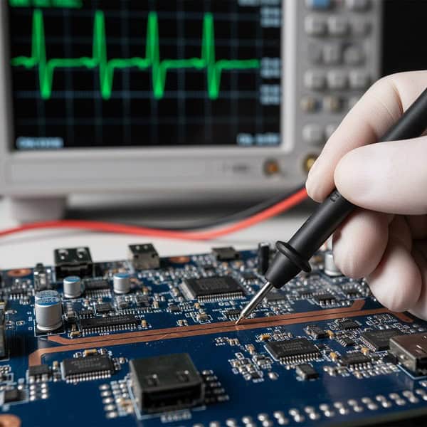
How to troubleshoot USB Pinout issues?
When a port fails, troubleshooting the USB Pinout usually involves checking for physical continuity, voltage levels, and signal integrity using an oscilloscope. Most issues stem from poor solder joints, reversed data lines, or inadequate grounding.
What should you check first?
You should always start with the power rails before diving into the complex data signals.
- Voltage Check: Is VBUS providing a steady 5V?
- Continuity: Use a multimeter to check for shorts between D+ and D-.
- Orientation: Ensure the connector’s footprint matches your PCB layout.
How do you diagnose data errors?
If power is present but data is not, the issue likely lies in the differential pair routing.
- Eye Diagrams: Used to check signal quality at high speeds.
- Reflections: Caused by impedance mismatches in the traces.
- Common Mode Noise: Often fixed with a common mode choke.
Key Takeaway: A systematic approach to checking your USB Pinout can save days of frustration during the IC programming and testing phase.
| Symptom | Likely Cause | Recommended Action |
| No Power | VBUS/GND short | Inspect solder joints |
| Device Not Recognized | D+/D- swapped | Cross-check schematic |
| Slow Data Speeds | Poor Shielding | Check cable quality |
Most hardware bugs are discovered and resolved by simply re-verifying the basic pin assignments against the datasheet.
What is the Mini USB Pinout used for today?
The Mini-USB USB Pinout is still found in many legacy and ruggedized applications where a sturdier connector than Micro-USB is required. While it lacks the high-speed capabilities of modern standards, its mechanical durability keeps it relevant in niche industries.
Is the pinout same as Micro-USB?
Yes, the electrical pinout is virtually identical to Micro-USB, including the 5-pin configuration.
- Pin 1: VBUS.
- Pin 4: ID (used for OTG in Mini-B).
- Pin 5: Ground.
- Mechanical Strength: Larger tabs make it harder to rip off the PCB.
Where will you still find it?
You will frequently encounter Mini-USB in professional audio equipment, industrial controllers, and telecom hardware.
- Legacy Support: Maintaining compatibility with older field equipment.
- Ruggedness: Preferred in environments with high vibration.
- Ease of Soldering: Larger pins are easier for manual rework.
Key Takeaway: The Mini USB Pinout remains a reliable choice for rugged hardware designed for long-term industrial use.
| Feature | Mini-USB | Micro-USB |
| Insertion Life | ~5,000 cycles | ~10,000 cycles |
| Size | Larger / Thicker | Thinner / Smaller |
| Strength | High | Moderate |
For projects where space is not the primary constraint, the physical robustness of Mini-USB can be a significant advantage.
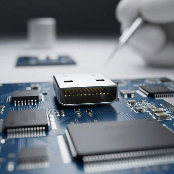
How to design a custom USB Pinout PCB?
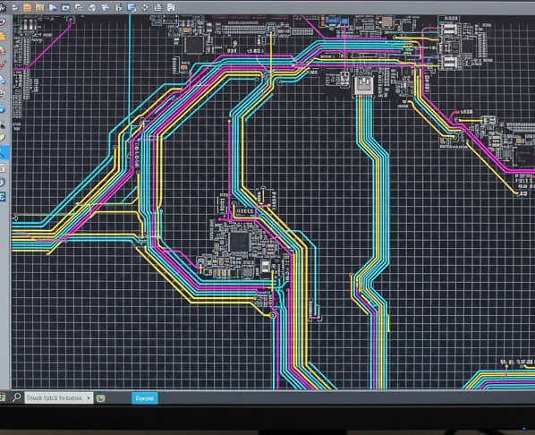
Designing a PCB with a USB Pinout requires strict adherence to layout rules to ensure the device is recognized by the host and operates safely. From the choice of the connector footprint to the routing of the 90-ohm differential pairs, every detail matters.
What are the layout “Golden Rules”?
You should follow these industry-standard practices to avoid common signal integrity pitfalls.
- Differential Routing: Keep D+ and D- traces parallel and equal in length.
- Ground Plane: Always route USB signals over a solid, unbroken ground plane.
- Stubs: Avoid any “T” junctions or stubs on high-speed data lines.
How to select the right partner?
Choosing a factory that understands these technical nuances is the difference between a working product and a pile of scrap.
- Design for Manufacturing (DFM): Ensuring the connector can be easily assembled.
- Experience: Look for partners familiar with high-speed digital design.
- Support: Engineers who can help you optimize your pinout for production.
Key Takeaway: A well-designed USB Pinout is only effective when paired with high-quality PCB assembly services.
| Design Stage | Critical Task | Potential Risk |
| Schematic | Pin Mapping | Connectivity failure |
| Layout | Impedance Control | Signal degradation |
| Assembly | Solder Quality | Intermittent connection |
Partnering with an experienced manufacturer ensures that your technical designs are translated into reliable, market-ready products.
Conclusion
Understanding the intricacies of the USB Pinout—from the simple 4-pin Type-A to the revolutionary 24-pin Type-C—is non-negotiable for modern hardware engineers. This guide has addressed the core challenges of signal integrity, power delivery negotiation, and connector selection that you face during the design phase. Whether you are building a simple charging device or a high-speed data hub, the accuracy of your wiring is the foundation of your product’s success.
At QueenEms, we don’t just assemble boards; we partner with you to solve complex engineering hurdles. If you are ready to bring your high-speed USB designs to life with a manufacturer that prioritizes precision and speed, contact us today to discuss your next project. Our mission is to transform your sourcing challenges into a scalable and dependable supply chain advantage.
FAQ
Can I use a USB 2.0 cable for USB 3.0 devices?
Yes, but with limitations. A USB 2.0 cable will only provide 480Mbps speeds and lower power delivery, as it lacks the additional 5 pins found in a USB 3.0 pinout.
What’s the best way to identify a Type-C pinout?
Look for the symmetrical 24-pin layout. The best way is to consult the specific datasheet for your connector, as different manufacturers may have slight variations in mounting tab positions.
How do I know if my USB wiring is correct?
Check for 5V on the VBUS pin and ensure there is no continuity between the data pins and ground. For high-speed designs, a signal integrity test with an oscilloscope is the gold standard.
Can I damage my device with an incorrect pinout?
Absolutely. Reversing the VBUS (+5V) and Ground pins is the most common way to permanently damage sensitive integrated circuits on your PCB.
What is the purpose of the ID pin in Micro USB?
The ID pin is used to trigger “OTG” mode. When grounded, it tells the device (like a phone) to act as a host and provide power to an external peripheral.