
Finding the correct orientation for your components is the first step in successful electronic manufacturing, but a single mistake in identifying the transistor pinout can lead to immediate circuit failure. Imagine receiving a batch of 500 assembled boards only to find that a “pinout-compatible” alternative was soldered backwards because the BOM data was ambiguous. This common nightmare for B2B buyers results in expensive rework and production delays. By mastering the nuances of pinout configurations, you can eliminate sourcing errors and ensure a seamless transistor pinout integration for your next project.
What Is a Transistor Pinout and Why Does It Matter for Assembly?
Basic-transistor-pinout-diagrams-for-NPN-and-PNP-types-with-labeled-Emitter-Base-and-Collector
A transistor pinout refers to the specific arrangement of the electrical leads (Emitter, Base, Collector, etc.) relative to the physical package of the component. You must understand that even transistors with the same electrical specifications can have different pin sequences depending on the manufacturer or package style.
How do we define the physical arrangement of leads?
The pinout is typically defined from the perspective of looking at the component’s front face or from the bottom. In professional PCB assembly, this definition dictates how the automated pick-and-place machine orientates the part.
- Standardization: While some packages have “common” layouts, there is no universal law.
- Visual Cues: Flat sides, tabs, or notches often indicate Pin 1.
- Documentation: The manufacturer’s datasheet is the only “source of truth” for pin mapping.
- Consistency: Sourcing from the same vendor ensures the layout remains identical across batches.
Why is pinout accuracy essential for electronic manufacturing?
If you provide an incorrect footprint based on a guessed pinout, the entire production run will be non-functional.
You might think a small-signal transistor is a simple part, but it is the most common cause of “dead on arrival” boards in mass production.
| Feature | Importance in Assembly | Impact of Error |
| Orientation | Directs pick-and-place logic | Reverse polarity / Short circuit |
| Footprint Match | Ensures solder joint integrity | Poor connectivity / Tombstones |
| Thermal Pad | Connects to PCB heat sinks | Component overheating |
Key Takeaway: Correct identification of Emitter, Base, and Collector is the first step in avoiding catastrophic board failures and ensuring long-term product reliability.
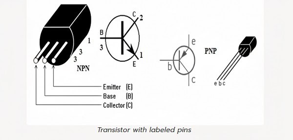
How Do You Identify BJT (Bipolar Junction Transistor) Pinouts?
Identifying BJT pinouts requires a clear understanding of whether you are dealing with an NPN or PNP type, as their functional leads are named Emitter (E), Base (B), and Collector (C). You will find that the physical sequence of these leads is the primary factor in your BJT pinouts verification process during BOM auditing.
What are the standard pinouts for NPN vs. PNP transistors?
Most through-hole BJTs like the TO-92 package follow a standard E-B-C or C-B-E sequence, but this varies globally.
- NPN Commonality: Many American parts use E-B-C, while Asian parts often use B-C-E.
- PNP Mirroring: PNP transistors often share the same physical footprint as their NPN counterparts.
- SOT-23 Leads: Surface mount versions typically have a triangular pin arrangement.
- Marking Codes: Small-signal BJTs use laser-etched codes to identify the specific part number.
Is there a universal rule for identifying these pins?
Unfortunately, there is no universal rule, which is why your assembly partner must verify the datasheet for every line item.
Have you ever wondered why two transistors with the same 2N2222 part number behave differently? It is often because the pinout changed between package variants!
| BJT Package | Pin 1 | Pin 2 | Pin 3 |
| TO-92 (Typical) | Emitter | Base | Collector |
| SOT-23 (Typical) | Base | Emitter | Collector |
Key Takeaway: Always cross-reference the datasheet with the physical package to ensure the E-B-C sequence matches your PCB footprint exactly.
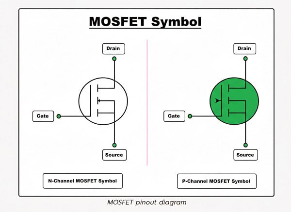
What Are the Key Differences in MOSFET Transistor Pinouts?
MOSFET pinout configurations differ fundamentally from BJTs because they use Gate (G), Drain (D), and Source (S) pins. When you are managing MOSFET assembly, understanding the voltage-controlled nature of these pins is vital for circuit safety.
How do Gate, Drain, and Source pins differ from BJT leads?
The Gate acts as the controller, the Drain is where the current enters, and the Source is where it exits.
- Static Sensitivity: The Gate pin is extremely sensitive to ESD.
- Internal Diodes: Most MOSFETs have an internal body diode between Drain and Source.
- Heat Dissipation: The Drain is often connected to the metal tab in power packages.
- Voltage Logic: Logic-level MOSFETs have specific gate thresholds that must be matched to the driver.
Why is ESD protection vital during the assembly process?
Because the Gate pin is insulated by a thin layer of oxide, a tiny static discharge can puncture it and ruin the part.
You must ensure your assembly factory uses grounded mats and wrist straps to protect these sensitive pin configurations.
| MOSFET Lead | Function | Assembly Risk |
| Gate (G) | Switching Control | ESD Damage |
| Drain (D) | Power Input | Thermal Overload |
| Source (S) | Common/Return | Ground Loops |
Key Takeaway: Unlike BJTs, MOSFETs are voltage-controlled and highly sensitive to static, requiring specific handling protocols and clean soldering.
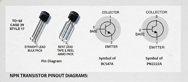
How Do Different Transistor Packages Affect Pinout Layouts?
The physical package, or “case,” is the biggest variable affecting the transistor pinout. You will see that as parts shrink from through-hole to surface-mount, the pin layout must adapt to the transistor pinout requirements of high-density boards.
How do SMT packages like SOT-23 differ from Through-Hole (TO-220)?
Through-hole packages like TO-220 are designed for power and easy identification, whereas SOT-23 focuses on saving space.
- Lead Spacing: SMT leads are much closer, increasing the risk of solder bridges.
- Tab Connectivity: In TO-220, the middle pin is usually internally connected to the metal tab.
- Height Profile: SMT packages allow for automated high-speed assembly.
- Standardization: SOT-23 is more standardized than TO-92, but variations still exist.
Can a single part number have different pinouts?
Yes, and this is a major pitfall for buyers sourcing from multiple vendors.
Don’t let a “low-cost alternative” ruin your production; check if the SOT-23 pin 1 is the same as your original spec!
| Package Type | Assembly Method | Common Application |
| TO-92 | Through-Hole | Small Signal / Prototyping |
| SOT-23 | Surface Mount | High-Density Consumer Electronics |
| TO-220 | Through-Hole | Power Supplies / Motor Control |
Key Takeaway: Package type dictates the PCB footprint; always verify that your supplier’s package code aligns perfectly with your design files.
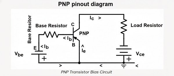
Why Is the NPN Transistor Pinout a Critical Sourcing Detail?
The NPN transistor pinout is the most frequently queried specification in industrial electronics. Since NPN transistors are used for ground-side switching, getting the NPN transistor pinout wrong can result in an “always-on” or “always-off” state that is hard to diagnose.
What is the most common pinout configuration for NPN?
While “E-B-C” is common for parts like the 2N3904, many power NPNs use a different order.
- Polarity: NPN requires a positive voltage at the base to turn on.
- Switching Logic: If pins are swapped, the transistor may act as a diode or fail.
- Package Dependency: TO-126 and TO-220 packages have very different NPN layouts.
- Industrial Parts: High-voltage NPNs often have wider pin spacing for insulation.
How to avoid the common mistake of reversing NPN leads?
The best way is to include a “pin 1” indicator on your PCB silkscreen and verify it against the component’s orientation marker.
It’s better to spend ten minutes checking a datasheet than ten days desoldering a thousand NPN transistors.
| NPN Part | Package | Pin Sequence (1-2-3) |
| 2N3904 | TO-92 | Emitter, Base, Collector |
| BC547 | TO-92 | Collector, Base, Emitter |
Key Takeaway: NPN transistors are the workhorses of switching circuits, and their pinout consistency is vital for high-speed automated assembly.
How Can You Verify Transistor Pinouts Using a Multimeter?
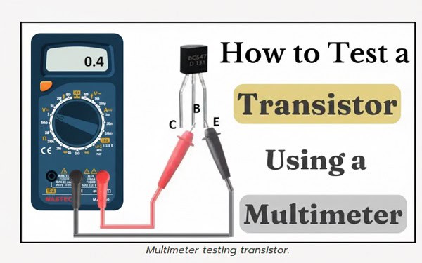
When you receive a batch of unlabelled components, verifying the transistor pinout manually is a necessary skill. You can use a digital multimeter’s diode test mode to confirm the transistor pinout before committing to a full production run.
What is the step-by-step process for diode testing a transistor?
By measuring the voltage drop between pins, you can identify the Base and determine if the part is NPN or PNP.
- Identify the Base: The pin that shows a reading with both other pins is the Base.
- Determine Type: If the red lead is on the Base, it’s NPN; if the black lead, it’s PNP.
- E vs C: The Emitter-Base junction usually has a slightly higher voltage drop than the Collector-Base.
- Open Circuit: A reading of “OL” in both directions indicates a blown junction or an FET.
How do engineers troubleshoot unknown configurations?
Engineers often use a “component tester” tool for instant pinout identification on the factory floor.
Have you ever been stuck with a reel of parts with no datasheet? A quick multimeter check is your best insurance policy.
| Test Leads | Reading (NPN) | Reading (PNP) |
| Base to Emitter | ~0.7V | OL |
| Base to Collector | ~0.6V | OL |
Key Takeaway: Manual verification is a valuable fail-safe for prototypes and incoming quality control before moving to full-scale manufacturing.
What Role Does the BOM Play in Transistor Pinout Accuracy?
Your Bill of Materials (BOM) is the communication bridge between your design and the factory floor regarding transistor pinout data. To ensure transistor pin configuration accuracy, you must provide more than just a part number.
How to structure your BOM to include specific pinout data?
A professional BOM should include the Manufacturer Part Number (MPN) and a link to the specific datasheet.
- Description Field: Explicitly state the package (e.g., SOT-23-3).
- Manufacturer: Different vendors might use different pinouts for the same generic name.
- Footprint Name: Use standardized naming conventions (e.g., TO-92_Inline_EBC).
- Substitution Rules: Note if pinout-compatible alternatives are allowed.
Why should you include datasheet links for every active component?
It allows the assembly engineer to quickly verify the orientation during the programming of AOI machines.
If you leave it to guesswork, you are essentially gambling with your production budget.
| BOM Column | Example Entry | Purpose |
| MPN | 2N2222A-BP | Specific component identification |
| Package | TO-92 | Physical layout constraints |
| Datasheet Link | [URL] | Final authority on pinout |
Key Takeaway: A detailed BOM minimizes communication gaps between your procurement team and the assembly plant, ensuring “Right First Time” production.
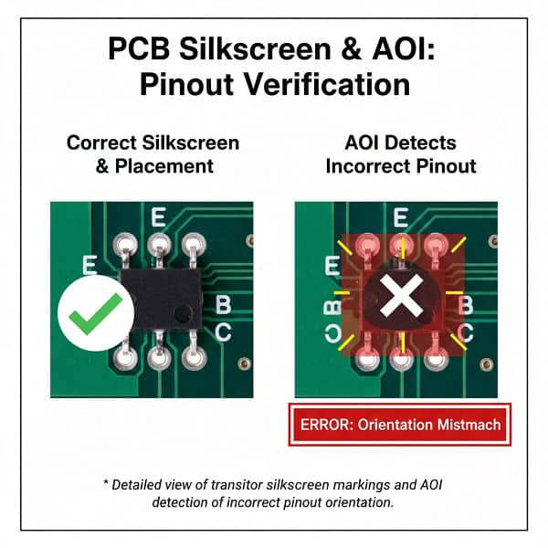
How to Prevent Assembly Defects Caused by Incorrect Pinouts?
Incorrect transistor pinouts lead to immediate failures, but they can be prevented through rigorous process control. In professional transistor pinouts management, we use technology to catch what the human eye misses.
What are the consequences of reversed pinouts in power circuits?
In power applications, a reversed transistor can explode or cause a fire due to uncontrolled current flow.
- Thermal Runaway: The part heats up instantly until it fails.
- Logic Errors: The circuit simply won’t switch, leading to “dead” boards.
- Adjacent Damage: High current through the wrong pin can fry the MCU or capacitors.
- Hidden Defects: Sometimes the part works poorly but fails after a few hours of use.
How do AOI (Automated Optical Inspection) systems detect orientation errors?
AOI cameras look for the polarity mark or laser-etched text to ensure the part matches the golden sample.
High-speed assembly is only as good as the inspection that follows it; you need both for mass production.
| Detection Method | Speed | Effectiveness |
| Visual Inspection | Slow | Low (Human Error) |
| AOI | Fast | High (Pattern Matching) |
| ICT (In-Circuit Test) | Moderate | Very High (Electrical Check) |
Key Takeaway: Proactive footprint checking and advanced inspection technologies are the dual pillars of defect-free PCBA in a professional factory environment.
Can You Interchangably Use Different Transistor Pinouts?
The biggest mistake a buyer can make is assuming that two transistors are interchangeable just because they share a package and a transistor pinout label. Even within the same transistor pinout category, electrical characteristics vary.
When is a “drop-in replacement” not actually a match?
Sometimes the pins are in the same order, but the gain (hFE) or voltage rating is different.
- Pin Mapping: One vendor’s “Pin 1” might be another’s “Pin 3.”
- Current Limits: Sourcing a lower-current version of the same pinout will lead to field failures.
- Switching Speed: Pinout-matched parts might be too slow for high-frequency PWM.
- Thermal Profile: Different lead materials affect how heat travels to the PCB.
What are the risks of using adapters in mass production?
Using pin-converter boards is acceptable for prototyping but is a major reliability risk for mass production.
You should always redesign the PCB footprint rather than forcing an incompatible pinout to fit.
| Factor | Drop-in Match | Functional Match |
| Pin Sequence | Identical | Can be different |
| Electrical Specs | Identical | Similar |
| Package Size | Identical | Identical |
Key Takeaway: Never assume two transistors are compatible just because they share the same package; electrical pinouts and internal specs vary wildly between manufacturers.
How to Optimize Your PCB Design for Reliable Transistor Pinout Assembly?
Your PCB layout is the final line of defense against transistor pinout errors. By designing for manufacturing (DFM), you make it easier for the transistor pin configuration to be verified during assembly.
Why are clear silkscreen markings essential?
Clear labels for “E”, “B”, and “C” (or G, D, S) allow manual inspectors to catch errors that machines might miss.
- Polarity Markers: Use a dot or a thick line to indicate Pin 1.
- Outline Drawings: The silkscreen should match the physical shape (e.g., the flat side of a TO-92).
- Labeling Leads: Don’t just number the pins 1-2-3; label their functions.
- Spacing: Ensure labels are not covered by the component body after soldering.
How does footprint spacing affect quality?
Tight spacing makes it harder to inspect the solder fillets and increases the chance of shorts between pins.
Have you noticed how high-quality boards always have clean, legible markings? It’s a sign of professional engineering.
| Design Element | Benefit to Assembly | User Usefulness |
| Functional Labels | Reduces manual inspection time | Easier troubleshooting |
| Precise Outlines | Ensures correct rotation | Prevents backward mounting |
| Thermal Vias | Improves heat dissipation | Extends product lifespan |
Key Takeaway: Good PCB layout practices make it impossible for assembly technicians and automated machines to get the orientation wrong, resulting in higher yields.
Securing Your Supply Chain with Technical Precision
Mastering the complexities of transistor pinout configurations is more than a technical requirement—it is a strategic advantage for any electronics brand. From ensuring your BOM is audited for pinout consistency to implementing advanced AOI and ICT testing, every step you take reduces the risk of costly production failures. This guide has addressed the critical pain points of component identification, sourcing accuracy, and assembly verification to help you achieve a defect-free product launch.
At QueenEMS, we understand that in high-precision PCBA, every lead matters and every micron counts. Our engineering-driven approach ensures that your transistor footprints are perfectly matched to your components, protecting your investment from the risks of reversed polarity or sourcing errors. Whether you are scaling a prototype or moving into high-volume mass production, we provide the technical oversight and manufacturing excellence your brand deserves. Contact us today to ensure your next production run is executed with flawless precision and industry-leading reliability.
FAQ
Can I use an NPN transistor if my PCB was designed for PNP?
No, you cannot swap them. Even if the transistor pinout sequence is identical, NPN and PNP transistors have opposite polarities and require different circuit configurations to function.
What’s the best way to find a datasheet for an old transistor?
Search for the full manufacturer’s prefix and the part number on reputable databases like Alldatasheet or DigiKey. If the markings are faded, a multimeter diode test is the best way to determine the pinout manually.
How do I know if my transistor is SMT or Through-Hole?
Check the package code on your BOM. Packages starting with “SOT” or “SOD” are surface-mount (SMT), while those starting with “TO”, “TIP”, or “DO” are typically through-hole components.
What is the most common mistake in transistor sourcing?
Relying on “typical” pinout diagrams rather than the specific manufacturer’s datasheet. Many generic parts have multiple pinout versions (e.g., 2N2222 in TO-92 can be EBC or CBE), so MPN verification is critical.