

SMT Assembly Process Explained: How Precision Manufacturing Enables Scalable and Reliable PCBAs
Managing complex electronic production often leads to significant manufacturing defects or delayed shipping schedules which frustrate procurement teams. Even a single failed solder joint might ruin entire batches, wasting thousands of dollars while damaging your hard-earned reputation with stakeholders. Utilizing a refined SMT Assembly Process ensures consistent reliability while lowering overall production expenses for your growing business. We maintain deep expertise in high-density electronics to guarantee every circuit board meets rigorous international standards.
SMT Assembly Process Explained: How Precision Manufacturing Enables Scalable and Reliable PCBAs
1. What is the SMT Assembly Process for high-performance electronics?
The SMT Assembly Process represents a sophisticated manufacturing method where electronic components are mounted directly onto the surface of printed circuit boards. This technique replaced older through-hole methods by allowing engineers to place smaller parts closer together. Here’s the deal, modern electronics demand extreme miniaturization that only surface mount technology provides. Most smart devices or industrial controllers rely on this workflow to achieve high processing power within tiny footprints.
What makes this method different?
Surface mounting eliminates the need for drilling many holes through every board layer. You will find that this reduction in mechanical drilling lowers fabrication costs significantly. But wait, there’s more, the lack of leads passing through the board frees up space on the opposite side for more components. This density improvement allows for complex routing that was previously impossible.
How does it benefit B2B buyers?
Procurement professionals value the scalability offered by automated surface mount lines. High-speed machinery places thousands of resistors or capacitors per hour with repeatable precision. Think about it, manual labor costs decrease while output quality remains stable across large production runs.
● Faster turnaround times
● Reduced board size requirements
● Lower unit costs at scale
Key Takeaway: Understanding this foundational method helps you design products that are easier to manufacture at lower costs.
SMT vs. Traditional Assembly
| Feature | SMT Process | Through-Hole |
| Component Size | Extremely Small | Large / Lead-based |
| Assembly Speed | High (Automated) | Slow (Manual/Wave) |
| Board Density | Very High | Low |
| Cost at Volume | Lower | Higher |
The table above illustrates why most industrial projects now prioritize surface mounting over older alternatives.
2. How does solder paste printing start the SMT Assembly Process?
The SMT Assembly Process begins with the precise application of solder paste through a stainless-steel stencil onto the PCB pads. This step acts as the foundation because the paste provides both the electrical connection and the mechanical glue during initial placement. What’s the real story? If the paste volume is inconsistent, the final board will likely suffer from “bridging” or “dry joints.” We use automated solder paste printers with integrated vision systems to verify alignment before every stroke.
Why is stencil quality so important?
Stencils are custom-made for your specific board design using laser-cutting technology. You need to ensure the aperture walls are smooth so the paste releases cleanly every time. Believe it or not, even a microscopic burr on the stencil can lead to uneven deposits. High-quality stencils prevent expensive rework later in the production cycle.
How do we control paste viscosity?
Solder paste consists of tiny metal spheres suspended in a flux medium. Temperature and humidity in the factory must remain constant to keep the material flowing correctly. The bottom line is, environmental control directly impacts the success of your PCBA project.
● Use of Type 4 or Type 5 solder powder
● Real-time stencil cleaning cycles
● Precise pressure control on squeegees
Key Takeaway: Investing in high-quality stencils and environmental control prevents 70% of common assembly defects.
Solder Paste Parameters
| Parameter | Optimal Range | Impact on Quality |
| Metal Content | 88% – 90% | Solder joint strength |
| Viscosity | 300 – 600 Kcps | Printing definition |
| Storage Temp | 2°C – 10°C | Shelf life and flux activity |
Careful management of these variables ensures the printing stage remains stable for thousands of cycles.
3. Why does SPI verify the SMT Assembly Process reliability?
The SMT Assembly Process incorporates Solder Paste Inspection (SPI) to catch errors before components are even placed on the board. This 3D scanning technology measures the volume, height, and area of every single paste deposit. Ready for the good part? Catching a printing error now costs cents, whereas fixing it after reflow soldering could cost hundreds of dollars. We use SPI to provide real-time feedback to the printing machine for automatic adjustments.
What does the 3D scan reveal?
Unlike 2D inspection, 3D SPI calculates the exact volume of the solder bricks. You can see if a pad has too little paste, which leads to weak joints. You might be wondering, does this slow down the line? Actually, modern SPI systems operate at line speed, ensuring no bottlenecks occur in your production.
How does data logging help you?
Every scan is recorded for traceability purposes in our quality management system. Here’s the deal, if a field failure occurs, we can look back at the exact paste profile of that specific serial number. This level of accountability is vital for medical or aerospace applications.
● Automatic rejection of bad boards
● Statistical Process Control (SPC) charts
● Offset detection for stencil alignment
Key Takeaway: SPI acts as a critical gatekeeper that ensures only perfect boards proceed to the expensive placement stage.
SPI Inspection Criteria
| Metric | Pass Condition | Potential Defect |
| Volume % | 80% – 120% | Insufficient solder or bridge |
| Height | 100um – 150um | Tombstoning risk |
| Area Cover | >95% of pad | Poor electrical contact |
Strict SPI thresholds prevent the majority of assembly-line escapes before they become permanent.
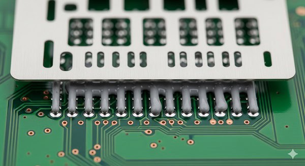
4. How do pick and place machines optimize the SMT Assembly Process?
The SMT Assembly Process utilizes high-speed robotic pick and place machines to position components with micron-level accuracy. These machines use vacuum nozzles to lift parts from feeders and place them onto the wet solder paste. This is where it gets interesting, a modern machine can place over 100,000 components per hour. You benefit from this speed through reduced lead times and lower labor costs on high-volume orders.
How is such high accuracy achieved?
Vision systems under the placement head photograph every component before it touches the board. The software calculates the center of the part and adjusts the rotation in milliseconds. It gets better, advanced sensors detect if a component is missing or tilted before placement occurs. This prevents the “empty pad” syndrome that plagues lower-quality manufacturers.
Can we handle odd-shaped components?
Flexible placement heads can swap nozzles automatically to handle everything from 01005 resistors to large BGA chips. You don’t have to worry about complex designs with mixed component sizes. The catch is, proper feeder setup is required to maintain this efficiency without interruption.
● Laser-guided alignment systems
● Multi-head parallel placement
● Intelligent feeder management
Key Takeaway: High-speed placement technology ensures your complex designs are assembled with perfect repeatability.
Placement Performance
| Component Type | Placement Speed | Accuracy Requirement |
| Small Chips (0201) | 50,000+ CPH | ± 30 micrometers |
| Large ICs / QFPs | 5,000+ CPH | ± 20 micrometers |
| BGA / CSP | 3,000+ CPH | ± 15 micrometers |
The machine’s ability to balance speed and precision determines the final yield of your PCBA.
5. What temperature profiles define the SMT Assembly Process reflow?
The SMT Assembly Process reaches its most critical thermal stage inside the reflow oven where the solder paste melts to form permanent bonds. The oven contains multiple heating zones that gradually raise the temperature of the entire assembly. What’s the catch? If the board heats up too fast, components might crack due to thermal shock. We carefully calibrate reflow profiles for every unique board thickness and component density.
What happens in the soaking zone?
The soaking zone allows all components to reach a uniform temperature before the final melting phase. You will notice that this prevents large parts from staying cool while small parts overheat. Think about it, achieving thermal equilibrium is the secret to avoiding cold solder joints in complex boards.
Why is the cooling phase important?
Controlled cooling ensures the solder crystallizes into a strong, fine-grained structure. But wait, there’s more, rapid cooling prevents the formation of brittle intermetallic layers. We use nitrogen-rich environments in some cases to further enhance joint integrity and prevent oxidation.
● Pre-heat, Soak, Reflow, and Cool zones
● Lead-free (RoHS) compatible profiles
● Real-time thermal profiling tools
Key Takeaway: A custom thermal profile protects your sensitive components while ensuring robust mechanical connections.
Reflow Profile Stages
| Zone | Target Temperature | Purpose |
| Pre-heat | 100°C – 150°C | Evaporate solvents |
| Soak | 150°C – 200°C | Activate flux |
| Reflow | 230°C – 250°C | Melt solder alloy |
| Cooling | 6°C/sec drop | Solidify joints |
Maintaining this curve is essential for passing long-term reliability tests in industrial environments.
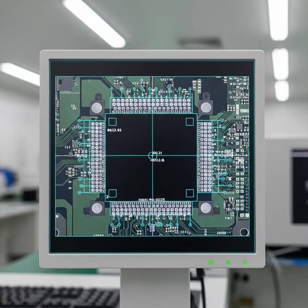
6. How does AOI technology inspect the SMT Assembly Process results?
The SMT Assembly Process relies on Automated Optical Inspection (AOI) to find defects that the human eye might miss. High-resolution cameras and multi-colored LED lighting systems capture images of every component from multiple angles. Here’s the deal, AOI identifies missing parts, incorrect polarity, and solder bridges within seconds. This automated check is mandatory for any professional-grade PCB assembly project.
How does the software identify defects?
The system compares the live image of your board against a “gold standard” or a library of component images. You can be sure that even a slightly skewed resistor will be flagged for review. Don’t forget, the software can also read part numbers to ensure the correct values were loaded onto the machines.
Why is 3D AOI superior?
Older 2D systems struggled with lifted leads or “tombstoning” where a part stands on one end. Modern 3D AOI measures the height of the solder fillets to confirm the joint volume is sufficient. The real story? 3D inspection reduces false calls while catching more real defects.
● High-speed image processing
● Multi-angle camera systems
● Database for defect trend analysis
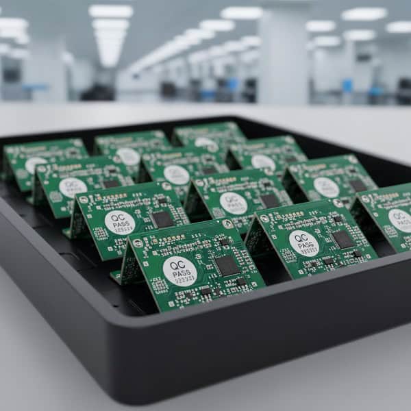
Key Takeaway: AOI provides a 100% inspection rate that manual labor could never achieve consistently.
AOI Detection Capabilities
| Defect Type | Detection Rate | Criticality |
| Missing Component | 100% | High (Fatal) |
| Solder Bridge | 99.9% | High (Short Circuit) |
| Polarity Error | 100% | High (Non-functional) |
This automated step ensures that only boards meeting your specifications move to the final testing phase.
7. Can X-ray scanning improve your SMT Assembly Process yields?
The SMT Assembly Process requires X-ray inspection for components like BGAs (Ball Grid Arrays) where the solder joints are hidden underneath the chip. Since cameras cannot see through the silicon, X-ray radiation is used to visualize the internal structure of the connections. This is where it gets interesting, we can detect “voiding” inside a solder ball that would otherwise cause intermittent failures. For high-reliability B2B products, X-ray is an essential quality assurance tool.
What are solder voids?
Voids are tiny air bubbles trapped inside the solder ball during the reflow process. You might find that too many voids weaken the connection and lead to cracks over time. Believe it or not, IPC standards allow for some voiding, but we aim for the absolute minimum to ensure product longevity.
How does it catch hidden bridges?
Sometimes solder flows between two balls under a BGA, creating a hidden short circuit. The bottom line is, without X-ray, you wouldn’t know why your board is failing until it reaches the end-user. We use 3D X-ray (CT scan) for particularly complex multi-layer boards.
● Non-destructive inspection
● Real-time void percentage calculation
● Inspection of buried vias and inner layers
Key Takeaway: X-ray inspection provides peace of mind for complex designs by “seeing” what is invisible to other tools.
X-ray Inspection Metrics
| Feature | Target Value | Risk |
| Voiding Ratio | < 25% (per IPC) | Mechanical failure |
| Ball Diameter | Uniform across grid | Open or short circuit |
| Alignment | Center of pad | Signal integrity issues |
Utilizing X-ray technology protects your investment by ensuring hidden connections are as perfect as the visible ones.
8. Why choose the SMT Assembly Process over traditional methods?
The SMT Assembly Process offers significant advantages in terms of electrical performance and manufacturing efficiency compared to through-hole technology. Because surface mount components have shorter leads or no leads at all, signal interference and inductance are greatly reduced. You might be wondering, is it worth the investment for simpler designs? Even for basic boards, the reduced size and automated assembly usually make SMT more cost-effective.
How does it impact signal integrity?
High-speed data circuits require very clean signal paths without the parasitic capacitance of long leads. You will see better performance in RF and high-frequency applications when using surface mount parts. Here’s the deal, at Gigahertz speeds, a through-hole lead acts like an antenna, causing noise issues.
Is the mechanical strength sufficient?
While through-hole joints are physically anchored in holes, modern SMT adhesives and solder alloys provide incredible bond strength. Think about it, your smartphone survives drops every day thanks to the durability of surface mount technology. For extremely heavy components, we often use a “hybrid” approach.
● Lower parasitic inductance
● Smaller PCB footprints
● Lower weight for aerospace/mobile use
Key Takeaway: Switching to SMT is the most effective way to improve both the performance and the profitability of your hardware.
SMT vs. THT Efficiency
| Metric | SMT Advantage | Business Impact |
| Component Cost | 20-40% cheaper | Lower BOM cost |
| Board Space | 60-80% smaller | Compact product design |
| Assembly Time | 10x faster | Faster time-to-market |
Choosing SMT allows you to stay competitive in an industry where speed and size are paramount.
9. What design rules facilitate a smooth SMT Assembly Process?
The SMT Assembly Process success depends heavily on Design for Manufacturing (DFM) principles followed during the PCB layout stage. Proper pad sizes, spacing, and thermal relief patterns prevent common assembly headaches like tombstoning or uneven soldering. Ready for the good part? A well-designed board can achieve 99% first-pass yields, saving you time and money. We offer free DFM reviews to all our B2B partners before production begins.
Why is component orientation critical?
If parts are oriented randomly, the reflow heat might hit one side before the other, causing the part to stand up. You should align components in the same direction to ensure uniform heating in the oven. But wait, there’s more, consistent orientation also makes AOI programming much faster and more accurate.
How do fiducial marks help?
Fiducials are small copper circles used by SMT machines to calibrate their position relative to the board. You might be wondering, can the machine just use the board edges? Edges can be inconsistent, but fiducials etched into the copper provide a perfect reference point every time.
● Standardized pad shapes (IPC-7351)
● Clear component silkscreen markings
● Proper solder mask clearances
Key Takeaway: Following strict DFM guidelines ensures your product can be mass-produced without constant technical hitches.
Common DFM Guidelines
| Rule | Requirement | Purpose |
| Fiducial Marks | 3 per board (global) | Machine alignment |
| Trace Width | Min 4-5 mils | Manufacturing yield |
| Clearance | Min 6-8 mils | Prevent solder shorts |
Proactive DFM analysis is the bridge between a theoretical design and a successful physical product.
10. How to select a partner for your SMT Assembly Process needs?
The SMT Assembly Process is only as good as the factory executing it, making your choice of PCBA partner the most important decision in the supply chain. You need a vendor that offers modern equipment, strict quality certifications, and transparent communication. The real story? A cheap vendor often ends up being more expensive due to hidden rework costs and late deliveries. We pride ourselves on being a partner that scales with your business needs.
What certifications should you look for?
ISO 9001 and IPC-A-610 are the industry benchmarks for quality management and workmanship. You should also check if the factory is RoHS compliant to ensure your products can be sold in international markets. It gets better, a partner with specialized certifications (like IATF 16949 for automotive) demonstrates a higher level of process control.
How important is technical support?
You don’t just want a “board stuffer”; you want an engineering team that catches errors before they happen. Bottom line, a partner that provides proactive feedback on your Bill of Materials (BOM) or layout saves you from costly production delays.
● Advanced equipment (3D SPI/AOI/X-ray)
● Transparent pricing with no hidden fees
● Fast-track prototyping services
Key Takeaway: The right partner acts as an extension of your own engineering team, ensuring every board is built for success.
Factory Evaluation Checklist
| Criteria | What to Look For | Why it Matters |
| Equipment | 3D AOI & X-ray machines | Quality assurance |
| Capacity | Multiple high-speed lines | Lead time reliability |
| Support | Dedicated project managers | Smooth communication |
Selecting a factory based on these metrics ensures your B2B operations remain efficient and risk-free.
Summary and Call to Action
The SMT Assembly Process is the backbone of the modern electronics industry, enabling the creation of powerful, compact, and reliable devices. By mastering each stage—from precision solder printing to advanced X-ray inspection—manufacturers can deliver high-quality PCBAs that meet the demands of today’s B2B markets. We have explored how automation drives consistency and how DFM rules prevent costly errors before they occur. Contact us today to discuss your next project and see how our precision manufacturing can help you scale your production with confidence. Our mission is to provide seamless assembly solutions that empower your brand to lead the industry with innovative hardware.
FAQ
Q1: Can I use SMT for high-power industrial applications?
Yes, SMT is perfectly suitable for high-power designs when using proper thermal management and heavier copper weights. Modern solder alloys and thermal vias allow surface mount components to dissipate heat efficiently even in demanding industrial environments.
Q2: What’s the best way to reduce SMT assembly costs for large orders?
The best way is to optimize your design for automated placement and use standard component sizes that are readily available. Reducing the number of unique parts on your BOM and ensuring your PCB is panellized correctly will significantly lower your per-unit manufacturing cost.
Q3: How do I know if my design is ready for the SMT Assembly Process?
You can confirm your design’s readiness by performing a comprehensive DFM (Design for Manufacturing) check. Most professional assembly partners provide this service to verify that pad sizes, component clearances, and fiducial marks meet the requirements of high-speed assembly lines.
Q4: Can I mix SMT and through-hole components on the same board?
Yes, this is called “hybrid assembly” and is very common for boards that require the strength of through-hole connectors alongside the density of SMT chips. While it adds a few steps to the process, it allows you to leverage the strengths of both technologies in a single product.
Q5: How do I choose between leaded and lead-free solder for my PCBA?
You should choose based on your target market’s regulations, as most regions now require lead-free (RoHS) compliance. Lead-free solder requires higher reflow temperatures and stricter process control, but it is the industry standard for modern, environmentally friendly electronics.