
Quick Answer: The right choice between pcb via tenting vs plugging vs filling depends on one thing: where your vias sit relative to your SMD pads. Via tenting (IPC-4761 Type II) costs nothing extra and protects general signal vias. Plugging (Type III/IV) adds 15%–30% to fabrication cost and is needed when vias sit within 0.5mm of BGA pads to prevent solder wicking. VIPPO (Type VII) adds up to +15%–20% to your total board cost and is maeasily adding 20% or morendatory only when vias land directly inside SMD pads — there is no cheaper substitute for that specific case.
Key takeaways:
- Tenting is free — it is the default solder mask process with no cost adder.
- Plugging (Type III/IV) adds 15%–30%; use it for vias within 0.5mm of BGA pads.
- VIPPO (Type VII) adds up to 20% of total board cost; mandatory for via-in-pad locations only.
- Writing “plug all vias” in your fab notes without an IPC type triggers an engineering hold — specify the type explicitly.
- Selective treatment saves 30%–50%: use Type VII only where needed, Type II everywhere else.
Table of Contents
- What Do PCB Via Tenting vs Plugging and Filling Actually Mean?
- What Does Each IPC-4761 Via Type Actually Cost?
- When Does Solder Wicking Actually Kill Your Assembly Yield?
- Is VIPPO Always Required for Via-in-Pad, or Can You Use a Cheaper Alternative?
- How Do You Specify PCB Via Tenting vs Plugging in Your Fab Notes?
- The 30-Second Decision Checklist: Which Via Treatment Does Your Board Need?
- Frequently Asked Questions About PCB Via Protection
You have finished your dense board layout and are ready to export your manufacturing files. You casually type “plug all vias” into your fab notes, expecting a standard build. A day later, your manufacturer places the entire order on engineering hold, asking if you mean IPC-4761 Type III, Type VI, or VIPPO — and your quick-turn prototype is now delayed.
After resolving hundreds of these exact engineering queries (EQs) last year, we know this confusion over pcb via tenting vs plugging costs hardware teams both time and budget. Choosing a via treatment is not a design preference; your component layout and assembly process dictate the exact standard you must follow. Here is the factory-floor reality of how to select and specify the exact IPC-4761 protection your board actually requires.
What Do PCB Via Tenting vs Plugging and Filling Actually Mean?
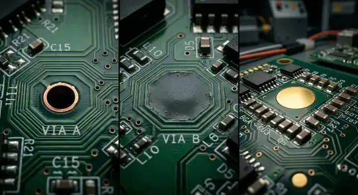
Understanding the physical difference between these treatments prevents costly manufacturing delays. Via tenting (IPC-4761 Type I/II) simply stretches liquid photoimageable (LPI) solder mask across the top of the via hole. Via plugging (Type III/IV) actively forces non-conductive epoxy partially into the via barrel. Via filling (Type V/VI) completely packs the barrel with epoxy, and VIPPO (Type VII) adds a flat copper cap over the filled hole.
The terminology gets severely confused on the production floor because many designers use “plugging” and “filling” interchangeably. They are entirely different mechanical processes. Tenting relies on the surface tension of standard solder mask. If the via diameter exceeds 0.3mm, the mask often breaks, leaving a tiny hole that traps corrosive chemicals during fabrication. Plugging uses a specialized machine to push thicker epoxy into the hole, creating a much stronger physical barrier.
Pull back the curtain on this… * Tenting (Type II): The most common and economical choice. Great for standard signal transitions.
- Plugging (Type IV): Recommended for vias near dense footprints where mask breakage would cause assembly defects.
- Filling & Capping (Type VII): The heaviest intervention, strictly reserved for complex high-density designs.
What Does Each IPC-4761 Via Type Actually Cost?
Via tenting costs $0 because it happens automatically during the standard solder mask application, while plugging adds 15% to 30% to your fabrication bill. Moving up to VIPPO (Type VII) is a massive price jump, easily adding +15% – 20% or more to your total PCB fabrication cost because it requires multiple extra baking, grinding, and plating steps.
You pay heavily for Type VII because the factory must fill the via with epoxy, bake it until hard, planarize (grind) the surface perfectly flat, and run the panel through the copper plating line a second time to create the cap. If you apply this rule to a standard board that does not need it, you are burning your budget. If you are comparing HDI vs standard PCB cost, the extensive use of filled and capped vias is exactly what drives the HDI price premium.
The practical reality is… you should match the treatment to the specific layout risk.
| IPC-4761 Type | Treatment Method | Cost Adder | Via Diameter Limit | Typical Application Scenario |
|---|---|---|---|---|
| Type I / II | Tenting (Single/Dual sided) | $0 Extra | < 0.3mm performs best | General signal vias, vias far from SMD pads |
| Type III / IV | Plugging (Single-sided recommended) | +15% – 30% | < 0.5mm | Vias near BGAs (0.35–0.5mm from pad) |
| Type V / VI | Filling (Non-conductive epoxy) | +30% – 50% | < 0.5mm | High-reliability industrial/medical designs |
| Type VII | VIPPO (Filled + Copper Capped) | +15% – 20% Total Board Price | < 0.5mm | Vias directly inside SMD pads (Mandatory for BGA pitch ≤0.65mm) |
Upload your Gerbers for a free DFM check — we flag via treatment conflicts before production starts, saving you 3–5 days of engineering queries.
When Does Solder Wicking Actually Kill Your Assembly Yield?
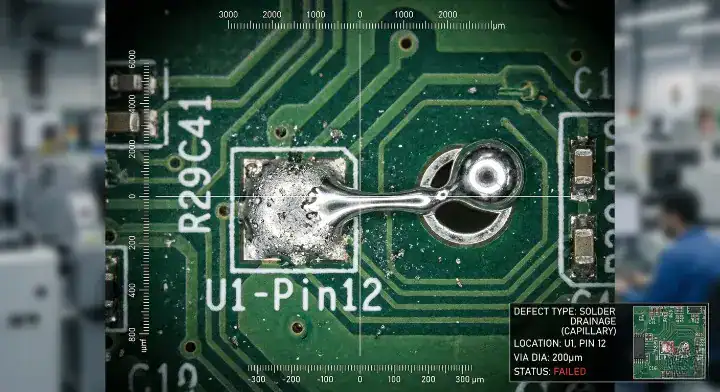
Solder wicking destroys your assembly yield when an untented or poorly plugged via sits closer than 0.35mm to an SMD pad. During the reflow oven cycle, the via barrel acts like a microscopic straw, utilizing capillary action to suck the molten solder paste off the adjacent pad, leaving your component with a weak cold joint or a complete open circuit.
Engineers frequently ask on forums: “Vias near symmetric pads are designed to wick solder — how do I prevent this from happening near BGA pads?” You prevent it by understanding the safe distance thresholds. When you route a dog-bone fanout for a BGA, the short trace between the pad and the via must be covered by solder mask. If the distance between the pad edge and the via hole drops below 0.25mm without proper tenting, you will see solder void rates skyrocket to 15%–30% based on our production data. Proper plugging drops that defect rate back to under 2%.
So what does this mean on the factory floor?
- Distance > 0.35mm: Standard Type II tenting is perfectly fine.
- Distance < 0.35mm: The mask dam will likely break. You must step up to Type IV plugging.
- Inside the pad: You have entered VIPPO territory.
Is VIPPO Always Required for Via-in-Pad, or Can You Use a Cheaper Alternative?
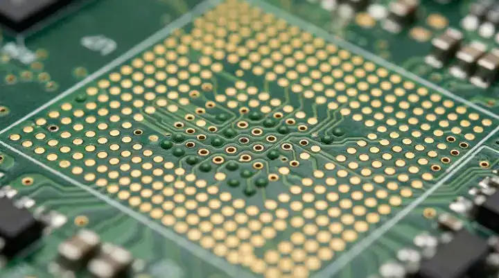
You must use Type VII VIPPO if the via hole is located completely inside the SMD component pad, but you can safely use cheaper tenting or plugging if you have enough space to use a standard dog-bone fanout. Many designers mistakenly pay for full VIPPO when a simple dog-bone trace would have worked flawlessly.
A common question we see is: “Do I always need full VIPPO for via-in-pad, or is there a cheaper option that still works?” The answer hinges entirely on your component pitch. At a BGA pitch of 0.8mm or higher, you almost always have the physical room to place the via outside the pad and connect it with a short trace. Once your BGA pitch drops to 0.65mm or below, geometry works against you. The dog-bone physically cannot fit, forcing you to place the via directly inside the pad. This requires HDI PCB manufacturing capabilities and makes VIPPO absolutely mandatory. You cannot substitute standard Type III plugging here, because the uneven epoxy surface will cause the BGA solder ball to sit unevenly, guaranteeing an assembly failure.
That said… smart layout practices save major capital.
- Selective VIPPO: Only specify Type VII for the specific BGA pad design locations that demand it.
- Hybrid approach: Use Type II tenting for the rest of the board. This specific strategy routinely saves our customers 30%–50% on via treatment costs.
How Do You Specify PCB Via Tenting vs Plugging in Your Fab Notes?
Writing vague instructions like “plug all vias” or “fill vias” in your fabrication notes is the fastest way to get your order put on an engineering hold. You must explicitly state the exact IPC-4761 Type number and specify which via sizes or locations receive the treatment.
Engineers complain: “My manufacturer keeps putting my order on hold because of ambiguous via plugging notes — what should I actually write?” Factories stop your job because guessing wrong ruins the board. If we assume you want Type II tenting but you actually needed Type VII VIPPO for a BGA, the entire batch will fail on the SMT line. You must provide clear instructions inside your Gerber file package, specifically on the fab drawing layer or in a dedicated readme text file.
Copy and paste these exact templates into your next fabrication drawing to significantly reduce engineering delays:
Template 1: Standard Tenting (Best for most standard designs)
“Via Treatment Note: All vias: IPC-4761 Type II (tented, both sides). No additional fill material required. Via mask clearance removed from all signal vias per layer$$X$$
of Gerber files.”
Template 2: Selective Plugging (Best for standard BGAs)
“Via Treatment Note: Vias within 0.5mm of BGA component pads (U1, U3, U7): IPC-4761 Type IV-a (plugged one side, covered with solder mask). Via locations identified in fabrication drawing Layer$$X$$
. All remaining vias: IPC-4761 Type II.”
Template 3: True Via-in-Pad (Best for fine-pitch HDI)
“Via Treatment Note: All via-in-pad locations as indicated in drill file$$filename.drl$$
: IPC-4761 Type VII (Via-in-Pad Plated Over / VIPPO). Non-conductive epoxy fill, planarized flush with copper surface, copper-capped and plated. Surface finish to match board standard. All other vias: IPC-4761 Type II.”
The 30-Second Decision Checklist: Which Via Treatment Does Your Board Need?
Match your specific layout geometry to the correct IPC-4761 standard using the matrix below. Never over-engineer your via protection — paying for filling when tenting works only drains your project budget without adding any electrical or mechanical benefit.
Not sure which IPC-4761 type your design needs? Send us your layout and we will review the via placements relative to your BGA pads for free.
| Your Board Scenario | Recommended Treatment | Reasoning |
|---|---|---|
| General signal vias, >0.5mm from SMD pads | Type II Tenting | Zero solder wicking risk, absolutely free. |
| Vias 0.35–0.5mm from BGA pad (dog-bone) | Type IV Plugging (Single-side) | Prevents wicking when mask dam is dangerously thin. |
| Vias <0.35mm from pad (but not inside) | Type VI Filling | Mask will break; requires complete sealing for safety. |
| Vias directly inside the SMD pad (Via-in-pad) | Type VII VIPPO — Mandatory | The only way to guarantee a flat surface for stencil printing. |
| BGA pitch ≥0.8mm with room for dog-bone | Type II Tenting | Avoids via-in-pad entirely, saving significant fabrication costs. |
| Medical/Industrial requiring extreme reliability | Type VI Filling (Whole board) | Meets harsh environment demands per IPC Class 3. |
| High-frequency RF boards | Type II Tenting | Hollow vias help control parasitic capacitance; epoxy changes electrical traits. |
Written by the QueenEMS Engineering Team. Ready to build your next board? Contact us today at https://www.queenems.com/
Frequently Asked Questions About PCB Via Protection
Can I use standard via tenting for via-in-pad designs?
No, it will ruin your assembly process. Standard tenting leaves a surface depression in the via-in-pad location. During stencil printing, solder paste volume over the depression is inconsistent, and during reflow the molten solder wicks into the open via barrel — leaving an insufficient joint or a complete open circuit. You must specify IPC-4761 Type VII (VIPPO) for any via located directly inside a component pad. Upload your design to QueenEMS, and we will verify your pad geometries for free.
Why does my manufacturer charge so much more for VIPPO?
VIPPO (Type VII) adds significant cost because it requires moving the panel back and forth across the factory floor multiple times. The factory must mechanically fill the vias with epoxy, cure them in an oven, use specialized equipment to grind the surface perfectly flat, and then run the board back through the copper plating baths to form the cap. This extra labor and machine time typically adds 15% to 20% to your fabrication bill. Contact us for a transparent quote to see exact pricing for your layer count.
What is the difference between via plugging and via filling?
Via plugging (Type III/IV) partially closes the via barrel to prevent solder wicking, usually pushing material in from one side. Via filling (Type V/VI) completely packs the entire depth of the via hole with epoxy, leaving no trapped air. Plugging is highly cost-effective for standard BGA fanouts, while filling is generally reserved for strict high-reliability applications like medical or aerospace devices.