
Quick Answer: The ideal PCB trace width spacing for stable, cost-effective manufacturing is 6mil/6mil. Pushing your design to a 4mil trace width spacing increases fabrication costs by 30% to 50% because it requires advanced HDI etching equipment, while dropping to 3mil doubles your board price. Key takeaways:
- 6mil traces yield a 98% manufacturing success rate; 5mil drops yield to 85% at budget fabs.
- Trace spacing should always be slightly larger than trace width to account for the etch factor.
- 1oz copper limits you to a 3mil minimum trace, while 2oz copper requires at least a 5mil trace.
- A 1A power trace needs roughly 10mil of width (at 1oz copper, 10°C rise), while 5A demands 80mil.
- What trace width and spacing should you actually use?
- What are the minimum trace width limits by copper weight?
- How does trace width affect your PCB fabrication cost?
- What spacing rules matter most for signal integrity?
- How do you calculate trace width for power traces?
- What can QueenEMS actually manufacture?
- FAQ
You just finished routing a dense microcontroller board with 4mil traces, feeling proud of the compact layout. Then, your manufacturer kicks the Gerber files back, claiming they cannot produce your PCB trace width spacing without charging double for HDI processing. Sound familiar? After processing thousands of PCB designs last year, we see engineers constantly guess the right trace parameters. Here is the exact data on what modern factories can actually produce, how your layout choices impact yield rates, and when to spend the extra money for tighter routing.
What trace width and spacing should you actually use?
You should use a 6mil trace width and 6mil spacing for the best balance of cost and manufacturing reliability. While factories can physically produce 3mil traces, operating at that extreme limit drops production yields and significantly raises your price per board.
But here’s what most guides won’t tell you… your trace spacing should ideally be slightly larger than your trace width. The chemical etching process removes copper from the sides of the trace, known as the etch factor. If you design a 5mil trace with exactly 5mil spacing, accidental over-etching or under-etching might cause tiny copper bridges (shorts). Giving the spacing a little extra breathing room prevents this defect.
| Routing Rule | Best Application | Cost Impact |
|---|---|---|
| 6mil / 6mil | Standard microcontrollers, budget boards | Lowest cost (Standard capability) |
| 5mil / 5mil | Fine-pitch QFNs, dense 2-layer vs 4-layer PCB | Slight premium |
| 4mil / 4mil | High-density digital signals | 30% – 50% more expensive |
| 3mil / 3mil | Advanced HDI PCB designs | 2x to 3x more expensive |
What are the minimum trace width limits by copper weight?
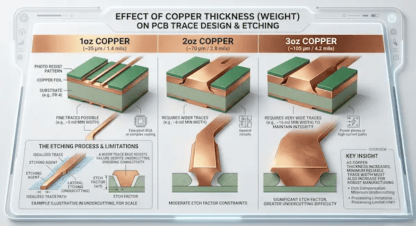
The minimum trace width for standard 1oz copper is 3mil, but this limit jumps to 5mil for 2oz copper and 9mil for 3oz copper. Thicker copper requires longer time in the chemical etching bath, which severely undercuts narrow traces and breaks the connection.
Here’s where it gets real… designers often forget that heavy copper and fine traces are natural enemies. If you try to run a 4mil signal trace on a layer pouring 3oz of copper for power distribution, the trace will literally wash away in the acid tank. You must separate your high-current layers from your fine-pitch signal layers. Read our guide on heavy copper PCB design to master these trade-offs.
| Copper Weight | Minimum Trace Width | Minimum Trace Spacing |
|---|---|---|
| 1 oz (35 µm) | 3 mil | 3 mil |
| 2 oz (70 µm) | 5 mil | 5 mil |
| 3 oz (105 µm) | 9 mil | 9 mil |
| 4 oz (140 µm) | 12 mil | 12 mil |
How does trace width affect your PCB fabrication cost?
Pushing your PCB trace width spacing below 6mil forces the factory to use expensive Laser Direct Imaging (LDI) equipment, increasing your total fabrication cost by up to 50%. Dropping below 4mil pushes your board into the high-density interconnect (HDI) category, instantly doubling your bare board price.
Now, here’s the part that surprises most customers… cheap traces cost you money in scrap. A client recently sent us a standard sensor board routed with 5mil traces and 5mil spaces. Their previous budget factory was giving them an 85% yield rate because the etch factor caused tiny shorts. We suggested changing the layout to 6mil/6mil. The yield jumped to 98%. They didn’t just save 1mil of board space; they saved 13% in scrap board costs.
Check out our PCB fabrication cost guide to see how these yields impact volume orders. As a general rule: if you have the physical space on the board, use a 6mil trace. Only shrink to 5mil or 4mil when BGA escape routing forces you to.
What spacing rules matter most for signal integrity?

You must apply the 3W rule for high-speed signals, keeping the spacing between traces at least three times the trace width to prevent crosstalk. For high-voltage lines, you must calculate creepage and clearance distances based on the specific voltage to prevent electrical arcing between exposed metal parts.
When routing differential pairs (like USB, PCIe, or HDMI), spacing dictates the impedance. You must use a PCB trace impedance calculator to hit that strict 90-ohm or 100-ohm target.
Want the honest answer? Do not just guess these numbers. Factory etching always alters the final geometry slightly. A 5mil trace on your screen might finish at 4.5mil on the physical board. Communicate your impedance targets clearly in your fab notes so the factory can apply the correct etch compensation.
How do you calculate trace width for power traces?
A 1-amp power trace requires approximately 10mil of width on a 1oz external copper layer to keep the temperature rise under 10°C. If you push 5 amps through the same board, you need a massive 80mil trace to prevent the copper from overheating and burning the FR4 material.
Internal layers trap heat, meaning a power trace buried inside a multilayer board needs to be almost twice as wide as an external trace carrying the exact same current. Stop relying on outdated forum charts and use our PCB trace width calculator (based on IPC-2152 standards) to get the exact millimeter value for your specific thermal limits.
| Current Load | External Layer Width (1oz, 10°C rise) | Internal Layer Width (1oz, 10°C rise) |
|---|---|---|
| 1A | ~10 mil | ~25 mil |
| 2A | ~25 mil | ~65 mil |
| 3A | ~40 mil | ~100 mil |
| 5A | ~80 mil | ~200 mil (Use a polygon pour) |
What can QueenEMS actually manufacture?
QueenEMS comfortably handles standard trace widths down to 4mil/4mil without severe cost penalties, and we push our extreme manufacturing limits down to 3mil/3mil for complex HDI projects. We provide a free DFM PCB design review on every order to verify your etch clearances before production begins.
Whether you are building simple prototypes or complex 60-layer telecommunication boards, you need a reliable multilayer PCB manufacturer who understands etch compensation.
If you are unsure where your design falls on the difficulty scale, do not wait until manufacturing fails. Upload your Gerbers to our portal. Our engineering team will flag high-risk trace spacing within 24 hours. Contact us today to get your free quote.
FAQ
Can I use different trace widths on the same layer? Yes, you should mix them. Signal lines can run at 6mil, while power lines on the exact same layer can run at 40mil. Just keep the overall copper density relatively balanced across the board to prevent warping during the reflow process.
Why do my 4mil traces keep breaking during manufacturing? You are likely using copper that is too thick. If you specify 2oz copper with 4mil traces, the acid etches away the sides of the trace faster than it cuts straight down, leading to a broken connection. Drop your copper weight to 1oz or half-ounce.
Should I use mil or mm for PCB layout? The global PCB manufacturing industry standardizes on “mils” (thousandths of an inch) for trace width and spacing, but uses millimeters for board dimensions and drill hole sizes. Stick to mils for your routing rules to match factory tooling directly.
Written by the QueenEMS Engineering Team