
Quick Answer: A PCB prototype failure usually stems from a disconnect between digital design software and physical manufacturing limits, costing hardware teams $3,000 to $15,000 per re-spin. Over 70% of first-run boards fail due to just seven preventable mistakes, ranging from ignoring factory spacing rules to ambiguous footprint data.
Key takeaways:
- DFM violations cause over 40% of physical board failures.
- A single wrong component footprint ruins the entire batch and adds 1-2 weeks of delay.
- Operating temperatures rising by 20°C cuts component lifespan by 50%.
- Skipping a pre-production factory review increases your average re-spins to 1.8 per project.
- Why does PCB prototype failure happen? The real numbers
- Reason 1 — DFM violations: your design worked in CAD but not on the factory floor
- Reason 2 — Wrong or unverified component footprints
- Reason 3 — Thermal design overlooked during prototyping
- Reason 4 — Incomplete or ambiguous manufacturing files
- Reason 5 — No test points or untestable design
- Reason 6 — Signal integrity issues not caught before layout sign-off
- Reason 7 — Skipping DFM review with the manufacturer
- FAQ
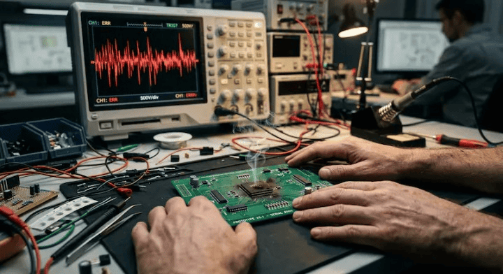
You open the shipping box, plug in your freshly assembled board, and… nothing happens. Or worse, you see the magic smoke. A single PCB prototype failure burns through four weeks of lead time and blows thousands of dollars from your hardware budget. After manufacturing over 3,000 prototype batches last year, we rarely see defects caused by the actual factory machines. Here is the honest breakdown of the seven design mistakes that trigger a physical failure, and the exact steps to intercept them before your next order.
Why does PCB prototype failure happen? The real numbers
PCB prototype failure happens primarily because engineers trust software defaults over physical factory capabilities, leading to an average of 1.8 re-spins per new hardware product. Fixing these errors before manufacturing costs nothing, while finding them after assembly adds $3,000 to $15,000 to your total PCB assembly cost.
Here’s where it gets real…
Hardware teams often assume the factory will catch their layout mistakes. Manufacturers build exactly what your files tell them to build. If you send flawed data, you get flawed boards.
Table 1: The 7 Core Causes of Prototype Re-spins
| Failure Reason | Trigger Scenario | Failure Probability | Cost Impact | Prevention Method |
|---|---|---|---|---|
| 1. DFM Violations | Spacing below factory limits | 40% | Full batch scrap | Load factory design rules early |
| 2. Wrong Footprints | 0402 part on 0201 pad | 25% | Batch scrap + 2 weeks | 1:1 IPC-7351B verification |
| 3. Thermal Issues | Overheats in enclosure | 15% | Redesign required | Thermal simulation |
| 4. File Ambiguity | Missing IPC-356 netlist | 10% | Inner layers reversed | Complete data package check |
| 5. No Test Points | Cannot debug the board | 5% | Blind re-spins | Add test pads to power rails |
| 6. Signal Integrity | High-speed data drops | 3% | Expensive lab debugging | Match trace impedances |
| 7. Skipping Review | Ignored factory feedback | 2% | Avoidable scrap | Pre-production DFM report |
Reason 1 — DFM violations: your design worked in CAD but not on the factory floor
Over 40% of prototype boards fail because the ECAD default Design Rule Check (DRC) parameters do not match the physical limitations of the chosen factory. Your software might allow a 4mil trace spacing, but if the factory’s standard etching limit is 6mil, the board will short out in the acid bath.
But here’s what most guides won’t tell you…
Your software DRC only checks math, not chemistry. A clean DRC run means absolutely nothing if you haven’t loaded the manufacturer’s specific rules. This is why DFM PCB design checks are a separate, necessary step.
- Ask your factory for their specific Design Rules file before you route the first trace.
- Import these exact parameters into Altium or KiCad.
- Pay close attention to minimum annular rings, as drill bits wander slightly during physical fabrication.
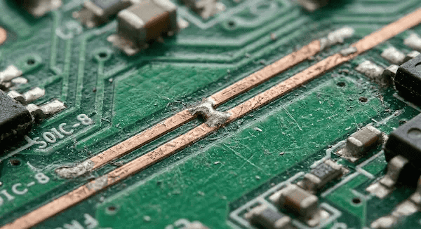
Reason 2 — Wrong or unverified component footprints
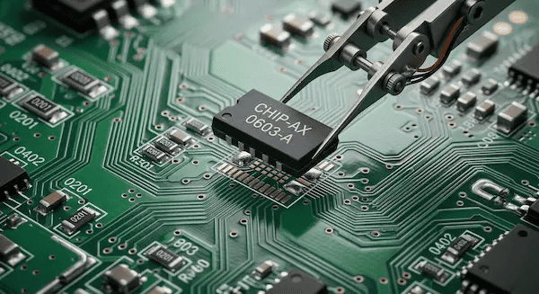
Footprint mismatches are the most expensive PCB prototype failure, forcing a 100% batch scrap when a component physically cannot sit on the copper pads. Writing “1k resistor” on your BOM instead of the full Manufacturer Part Number (MPN) forces the factory to guess, often resulting in a 0402 part being placed on a 0201 pad.
Now, here’s the part that surprises most customers…
You cannot fix a footprint error with a software patch. If the microcontroller pinout is reversed, the physical board is completely dead.
- Always write out the full, 15-character MPN in your BOM for PCB assembly.
- Watch out for ambiguous polarity markings on diodes and tantalum capacitors.
- Use IPC-7351B standard footprint libraries rather than drawing custom pads from scratch.
Reason 3 — Thermal design overlooked during prototyping
Thermal-related prototype failures happen because boards pass a quick 10-minute bench test in an air-conditioned room, but overheat and die when running continuously inside a closed plastic enclosure. Industry data shows that for every 20°C rise in operating temperature, the lifespan of your electronic components drops by half.
The real question is…
Did you test the board exactly how the end-user will treat it? Bench tests create a false sense of security.
- Space out high-power components; grouping voltage regulators together creates dangerous hotspots.
- Add thermal vias under high-heat ICs to pull heat down into the internal ground planes.
- Use a thermal camera during your initial prototype boot-up to physically verify your heat dissipation strategy.
Reason 4 — Incomplete or ambiguous manufacturing files
Submitting incomplete data packages forces the CAM engineer to make assumptions, amplifying a small documentation gap into a fatal manufacturing error across the entire batch. If you omit the IPC-356 netlist, the factory cannot electronically verify your layout against your schematic and must rely on visual checks.
So what does this actually mean for your budget?
File problems are silent killers. The factory might not tell you they guessed your layer stack-up until the inner copper layers arrive reversed. Your prototype is dead on arrival.
- Always include a clear, text-based layer stack-up guide in your export.
- Separate your plated through-hole (PTH) and non-plated (NPTH) drill files.
- Double-check what PCB assembly quote files do you actually need to stop the factory from guessing.
Reason 5 — No test points or untestable design
Failing to include accessible test points turns a simple debugging session into a blind guessing game, directly increasing your chances of needing multiple re-spins. Without physical access to critical signal lines, you cannot locate the root cause of the PCB prototype failure.
Want the honest answer?
If you cannot probe it, you cannot fix it. You will end up guessing what went wrong, changing the design blindly, and hoping prototype version 2 works.
- Place designated test pads on every single power rail and ground connection.
- Keep test points away from tall components like large electrolytic capacitors so your oscilloscope probes actually fit.
- Put all test points on the bottom layer if you plan to use a pogo-pin test fixture in the future.
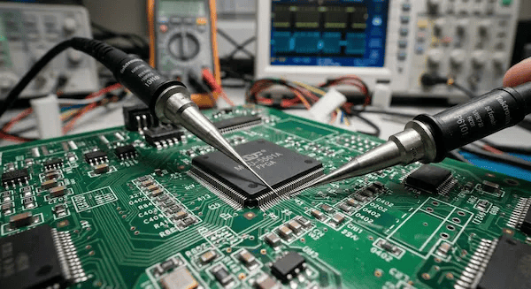
Reason 6 — Signal integrity issues not caught before layout sign-off
Signal integrity degradation causes intermittent board resets and data drops, usually triggered by improper impedance matching or poor return paths in high-speed circuits. These invisible failures pass all basic continuity tests at the factory but crash your firmware randomly during real-world operation.
It all comes down to this…
A physical short circuit is easy to find. A bouncing ground plane due to a high-speed switching trace is a nightmare to debug.
- Maintain a solid, unbroken ground plane directly beneath your high-speed data lines.
- Match your trace lengths precisely for differential pairs like USB or HDMI.
- Avoid via stubs in high-speed routing, as they act like tiny antennas that bounce signals back and forth.
Reason 7 — Skipping DFM review with the manufacturer
Bypassing the factory’s pre-production DFM PCB design review is the easiest mistake to make, directly responsible for pushing the average project from one prototype run to nearly two. Let the people building the board review the files before they cut the fiberglass.
Here’s the bottom line from the factory floor:
- Every week, we see customers complain that their board failed despite passing their local DRC. The most common trigger is using ECAD default rules rather than our actual physical capability parameters.
- At QueenEMS, we send every new customer our specific PCB Design Rules file before they start routing. Once you submit files, we run them through our system and deliver a free, actionable DFM report within 2 hours.
- Customers who modify their layout based on our DFM report hit a first-pass yield of over 95%. Customers who skip this step average 1.8 re-spins before reaching mass production.
Table 2: First-Pass Success Checklist (Check Before You Export)
| Category | Verification Step | Status |
|---|---|---|
| Design Rules | Replaced ECAD defaults with chosen factory’s rules | [ ] |
| Footprints | Verified 1:1 against the physical component datasheet | [ ] |
| BOM Match | Every MPN exactly matches the schematic symbol | [ ] |
| Testability | Added exposed test points on all voltage rails | [ ] |
| File Export | Included IPC-356 netlist and exact layer stack-up | [ ] |
FAQ
Can the factory fix a component footprint error after the board is made? No. If the copper pads on the bare board are too small or spaced incorrectly for the physical component, the automated SMT machines cannot place the part. Manual soldering workarounds are sometimes possible for prototypes, but they are highly unreliable and ruin the board’s integrity.
How many prototypes should I order for the first run? For a completely new design, ordering 5 to 10 boards is the standard practice. This gives you enough units to run bench testing, thermal testing, and firmware debugging simultaneously without wasting thousands of dollars if a major flaw forces a re-spin.
Does a higher layer count increase the risk of failure? Yes. Moving from a 4-layer to an 8-layer board increases manufacturing complexity. Registration errors between internal layers become more common, and blind/buried vias introduce physical risks that do not exist on simpler boards. Always request a free DFM check when pushing past 4 layers.
Checked these 7 reasons against your next design? Upload your Gerber files today. QueenEMS engineers will run a free DFM check to intercept these issues before your board hits the factory floor, not after. Get started with your turnkey PCB assembly at QueenEMS.
Written by the QueenEMS Engineering Team