
Quick Answer: Standard PCB fabrication lead time typically ranges from 3 to 15 business days, dictated heavily by your board’s layer count and material specifications. A simple 2-layer FR4 prototype takes 3–5 days, while complex 8+ layer boards with HDI features require 10–15+ days just for bare board production.
Key takeaways:
- Fabrication time excludes weekends, holidays, engineering review (1–2 days), and transit.
- Specifying green solder mask and HASL finish saves 1–3 days compared to custom colors or ENIG.
- Blind or buried vias add 3–5 days to your schedule because they require multiple lamination cycles.
- Rush services can cut production time by half but carry a 20–50% price premium.
- What is PCB fabrication lead time and how is it counted?
- How long does PCB fabrication take by layer count?
- What are the stages of PCB production and how long does each take?
- What design choices slow down your delivery?
- How can you shorten lead time without paying rush fees?
- When is quick-turn PCB worth the extra cost?
- FAQ
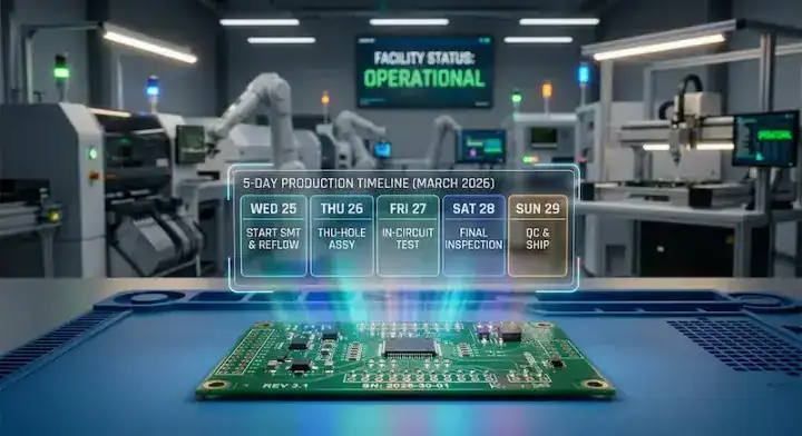
You submitted your Gerber files on a Tuesday, expecting bare boards on your desk by Friday, only to receive an automated notification pushing your ship date two weeks out. Sound familiar? Hardware teams frequently underestimate PCB fabrication lead time, stalling entire product launch schedules over a single misunderstood specification. After processing over 12,000 PCB orders last year, we see this confusion constantly. Here is exactly what drives those timelines on the factory floor—and how to get your boards faster without relying on expensive rush fees. Just keep in mind this guide covers bare board manufacturing only; your total project schedule must also factor in PCB assembly cost and component sourcing time.
What is PCB fabrication lead time and how is it counted?
PCB fabrication lead time is the specific number of working days a factory needs to manufacture your bare boards, beginning only after engineering files are approved and materials are secured. This production clock runs strictly Monday through Friday, completely ignores national holidays, and stops the moment your boards hit the shipping dock. Your actual delivery day will always be later than the fabrication completion date.
Here’s the part that surprises most customers…
Many engineers assume the clock starts the second they hit “upload.” It doesn’t.
- The CAM delay: The timer begins after the factory completes their CAM (Computer-Aided Manufacturing) review and you resolve any EQ (Engineering Queries).
- Business days only: Weekends halt the clock. A “5-day lead time” starting on Thursday means your boards ship the following Wednesday.
- Quick-turn defined: Standard quick-turn generally refers to delivery under 20 business days. For prototypes, true quick-turn means 24 hours to 5 days.
- Shipping is separate: Fabrication time does not include transit. Next-day air vs. standard ground significantly alters your total wait.
To avoid delays right at the starting line, review exactly what PCB assembly quote files you actually need before submitting your package.
How long does PCB fabrication take by layer count?
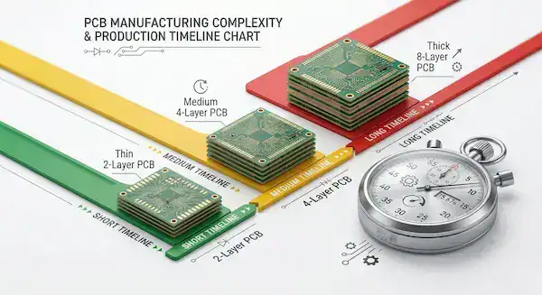
A standard 2-layer PCB requires 3–5 business days to fabricate, a 4-layer board takes 5–7 days, a 6-layer needs 7–10 days, and anything 8 layers or above demands 10–15+ days. These baseline estimates assume standard FR4 materials without complex HDI features. Factory scheduling revolves entirely around lamination cycles, meaning more layers directly force your board through more trips in the heating presses.
So what does this actually mean for your schedule?
We mapped out the typical timelines based on real factory data across different volume tiers:
| Layer Count | Prototype (5–50 pcs) | Small Batch (100–500 pcs) | Mass Production (1000+ pcs) |
|---|---|---|---|
| 2-Layer | 3–5 Days | 5–7 Days | 7–10 Days |
| 4-Layer | 5–7 Days | 7–10 Days | 10–14 Days |
| 6-Layer | 7–10 Days | 10–12 Days | 14–18 Days |
| 8+ Layers | 10–15+ Days | 15–20 Days | 20–25+ Days |
If your timeline is tighter than these standard estimates, our rapid PCB prototyping service can compress these numbers for standard designs.
What are the stages of PCB production and how long does each take?
Bare board production breaks down into five primary stages: engineering review (1–2 days), material preparation (0–5 days), physical fabrication (3–10 days), electrical testing (1–2 days), and packaging (1 day). Your board spends the bulk of its life physically transferring between chemical etching baths, lamination presses, and mechanical drilling stations.
But here’s what most guides won’t tell you…
30% of delayed prototype orders get stalled before they even touch a machine.
We constantly see designers submit files missing explicit stackup definitions or drill charts. The factory stops everything to issue an Engineering Query. We built a free DFM/DFA engineering review on every order that flags missing assets immediately. This proactive check cuts our average quote-to-production time from 4 days to under 24 hours.
- Engineering Review (1–2 Days): CAM engineers translate your Gerbers into machine code and verify tolerances.
- Material Prep (0–5 Days): Standard FR4 is pulled immediately. Exotic high-frequency Rogers materials require procurement time.
- Fabrication (3–10 Days): The heavy lifting. This involves imaging, etching, pressing, drilling, and plating.
- Testing & Inspection (1–2 Days): Flying probe testing for small runs; bed-of-nails fixtures for larger batches.
- Packaging (1 Day): Vacuum sealing and final boxing for dispatch.
What design choices slow down your delivery?
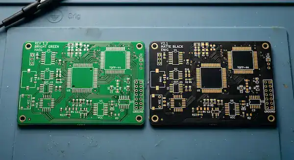
Specifying non-standard features like black solder mask, ENIG surface finish, or blind/buried vias adds anywhere from 1 to 5 days to your total PCB fabrication lead time. Factories highly optimize their main production lines for green solder mask and standard through-holes. Any deviation forces your boards onto slower, specialized batch processing lines.
Let’s look at the actual numbers…
Every custom specification pulls your board off the high-speed line.
| Design Feature | Fastest Option | Slower Option | Added Lead Time | Why it slows you down |
|---|---|---|---|---|
| Solder Mask | Green (Factory Default) | Black, White, Matte | +1–2 Days | Demands line changeovers and altered UV curing times. |
| Surface Finish | HASL / Lead-Free HASL | ENIG, Hard Gold | +0.5–1 Day | ENIG requires complex electroless chemical plating baths. |
| Via Type | Standard Through-Hole | Blind / Buried Vias | +3–5 Days | Needs sequential lamination (pressing and drilling multiple times). |
| Impedance | Standard Traces | Controlled Impedance | +1–2 Days | Requires custom test coupon generation and TDR verification. |
Understanding these trade-offs helps you predict your PCB fabrication cost and delivery date simultaneously.
How can you shorten lead time without paying rush fees?
You can slash 2–5 days off your timeline for free by submitting flawless files, defaulting to standard green FR4, and utilizing factories that warehouse their own materials. Clean data allows CAM engineers to skip the back-and-forth EQ process and release your board directly to the floor. Smart hardware teams optimize for manufacturability to naturally accelerate the line.
Want the honest answer?
You don’t always need to open your wallet to go faster.
- Submit complete documentation: Provide intact Gerbers, clear drill charts, and an unambiguous stackup text file.
- Use standard materials: Specify common Tg ratings. Factories keep tons of standard FR4 in stock, avoiding supplier delays.
- Pre-panelize your design: If you know the factory’s standard panel dimensions, setting up the array yourself saves CAM engineers hours of prep work.
- Communicate early: Tell your manufacturing partner your target dates before you finalize the BOM for PCB assembly. We can reserve capacity on our drilling machines if we know your files are dropping on Friday.
We noticed customers choosing exotic Tg FR4 for simple consumer boards, causing 2-week material procurement delays. We standardized on high-quality Tg150 and Tg170 for our regular inventory. This move eliminated material wait times for 92% of our standard prototype orders.
When is quick-turn PCB worth the extra cost?
Paying a 20–50% premium for quick-turn fabrication makes sense when missing a product launch window, trade show deadline, or investor demo costs your business significantly more than the expedite fee. Quick-turn services compress a standard 10-day cycle into under 5 days by prioritizing your job at every single factory station. It functions as an insurance policy for your master schedule.
The real question is…
Are you saving pennies just to burn dollars downstream?
- Failing fast: Validating a risky sub-circuit on a 48-hour mini-board saves weeks of downstream debugging on the main layout.
- Component shelf life: If you secured allocation on hard-to-find chips for quick turn PCB assembly, delaying the bare boards might force you to lose your slot on the SMT line.
- The premium is a range: Expect a 20% markup to shave a couple of days, scaling up to 50% or more for true 24-hour turns.
Your exact price always depends on your specific design complexity. Upload your Gerber package to get a precise quote.
FAQ
Can I get an 8-layer board fabricated in 24 hours? No. Physics prevents this. An 8-layer board requires multiple pressing and curing cycles that take more than 24 hours just to heat and cool properly. The fastest realistic turn for an 8-layer board is typically 3–4 days under extreme expedite conditions. Get a transparent quote within 24 hours to see the fastest standard options for your specific stackup.
Does my shipping method affect the fabrication lead time? It depends on how you define your schedule. Fabrication lead time strictly stops when the boards are boxed at the factory. However, choosing overnight air instead of standard ground drastically reduces your total delivery timeline. Always clarify transit methods when reviewing quotes to align your expectations.
What happens if the factory finds a design error on day 2? The production clock stops immediately. The factory will issue an Engineering Query (EQ), and the lead time counter will not resume until you provide a corrected file or written approval to proceed. Upload your BOM and Gerbers for a free DFM check before ordering to prevent this exact scenario.
Written by the QueenEMS Engineering Team. Ready to finalize your production schedule? Contact us today to get a precise timeline for your next project.