
Quick Answer: The most common PCB fabrication defects range from cosmetic solder mask blistering to catastrophic delamination that can scrap entire production batches, wasting $500 to $2,000+ per order. Catching these flaws early requires strict DFM analysis and inspecting your bare boards for warping and exposed copper before surface mount assembly begins. Key takeaways:
- Delamination and galvanic corrosion are fatal manufacturing defects that require completely scrapping the board.
- Insufficient annular rings account for 28% of all DFM warnings and cause 5x more via fractures during production.
- Light board warping under 0.75% passes IPC Class 2 standards, but anything over 1.5% will jam SMT machines.
- Running a free DFM check catches 80% of design-induced fabrication errors before you pay for tooling.
- What are the most common PCB fabrication defects?
- Which defects are caused by design vs. manufacturing?
- How do these defects affect your product reliability?
- How can you prevent defects in your PCB design?
- What should you check when you receive your PCBs?
- FAQ
You just opened a box of freshly manufactured circuit boards, and the green solder mask is already peeling off the edges. If you send these questionable boards down the SMT line, you risk ruining thousands of dollars in expensive microchips on a faulty foundation. After running quality control on over 4,500 PCB batches last year, we know exactly what a bad board looks like straight out of the vacuum bag. Here is a factory engineer’s guide to identifying the top fabrication defects, figuring out who is at fault, and preventing them from ruining your next order.
What are the most common PCB fabrication defects?
The top PCB fabrication defects include delamination, warping, and BGA solder voids, which directly cause electrical shorts or open circuits. Understanding these specific failure modes helps you quickly determine if a bad batch was caused by poor layout routing or sloppy factory etching.
Here’s where it gets real… many designers blindly blame the factory for every bad board. Sometimes the fabricator leaves the boards in the etching acid too long. Other times, your trace spacing was mathematically impossible to manufacture safely.
Here are the top 10 defects, what they look like, and who typically takes the blame:
| Defect Name | What It Looks Like | Primary Cause | Responsibility | Cost Impact |
|---|---|---|---|---|
| Delamination | Bubbles or separation between FR4 layers | High moisture or severe thermal shock | Both | Scrap entire board ($500+) |
| Poor Solderability | Solder refusing to wet the copper pads | Oxidized or contaminated surface finish | Manufacturing | Rework joints ($200+) |
| Warping | Board bows or twists on a flat table | Unbalanced copper or thin core | Both | SMT failure ($1000+) |
| Exposed Copper | Missing solder mask over traces | Mask peeling or artwork misalignment | Manufacturing | High short risk ($300+) |
| BGA Solder Voids | X-ray shows empty air inside joints | Poor outgassing or bad reflow profile | Manufacturing | Expensive rework ($800+) |
| Solder Mask Blistering | Flaking or bubbling green mask | Surface contamination before coating | Manufacturing | Scrap board ($150+) |
| Via Fill Defects | Dimples or empty voids in plugged vias | Trapped air during the plating process | Manufacturing | Broken connections |
| Dimensional Deviations | Board doesn’t fit inside your enclosure | Loose CNC routing tolerances | Manufacturing | Scrap batch |
| Galvanic Corrosion | “Black pad” under ENIG surface finish | Excessive phosphorus in the nickel bath | Manufacturing | Total PCBA failure |
| Impedance Failures | USB/PCIe signals dropping out constantly | Incorrect trace width or poor etching | Both | Complete redesign |
Read our detailed breakdown of PCB warping causes if your boards look like potato chips.
Which defects are caused by design vs. manufacturing?
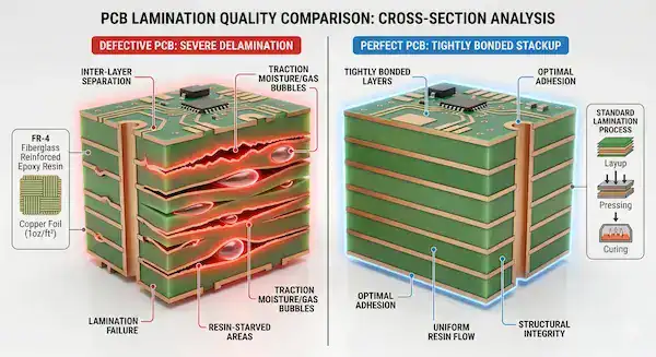
Manufacturing defects like galvanic corrosion and solder mask blistering are 100% the factory’s fault, while warping and impedance failures are often shared responsibilities. If you submit a perfectly balanced Gerber file with safe clearances, any subsequent physical flaws fall squarely on the manufacturer’s quality control team.
But here’s what most guides won’t tell you… a defect is only a defect if it violates your chosen standard. According to industry guidelines, minor cosmetic scratches on the solder mask might pass a standard inspection. If you require absolute perfection, you must specify strict acceptance criteria upfront. We highly recommend reading our guide on how to choose the right IPC standards to understand what flaws Class 2 accepts that Class 3 rejects outright.
How do these defects affect your product reliability?
A single fabrication defect like a cracked via can turn a functioning prototype into a dead brick after just three weeks in the field. Ignoring a high defect rate during bare board production mathematically guarantees massive field returns once the product hits the hands of your customers.
When trace width limits are ignored, over-etching creates micro-breaks that act like blown fuses under high current. This drives up your overall PCB fabrication cost because you are paying full price for scrap material.
How can you prevent defects in your PCB design?

You can prevent major fabrication defects by balancing your copper layers symmetrically, keeping trace clearances above 5mil, and defining proper solder mask openings. Running these parameters through an automated checker stops etching failures before you ever pay for tooling charges.
We see engineers make the same layout mistakes daily. Last year, the #1 design issue we found during our DFM PCB design checks was insufficient annular ring—accounting for 28% of all feedback. If left unfixed, the probability of via fracture during production is 5 times higher.
To protect your next design from factory rejection, follow these rules:
- Fix your vias: Calculate your drill sizes correctly. Review our annular ring guide to prevent drill breakouts.
- Widen your traces: Stop routing 3mil lines unless absolutely necessary. Stick to safe limits shown in our PCB trace width spacing guide.
- Check your mask: Prevent exposed copper and bridges by understanding what is solder mask expansion.
What should you check when you receive your PCBs?
When you receive a new batch of bare boards, you should perform a 5-step unboxing check involving visual inspection, caliper measurements, and multimeter continuity testing. Catching a fabrication error before sending the boards to the SMT line saves you from wasting expensive microchips on dead fiberglass.
Now, here’s the part that surprises most customers… you don’t need a million-dollar lab to do basic incoming quality control (IQC). You can spot 90% of severe factory errors right at your desk.
Run through this 5-step unboxing checklist immediately:
- Visual Scan: Hold the board at an angle under bright light. Look for warping, surface discoloration, deep scratches, or flaking mask.
- Dimension Check: Grab digital calipers. Measure the outer board edges and check three different mounting hole diameters.
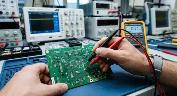
- Multimeter Test: Set your meter to continuity mode. Probe your main power rails to check for dead shorts.
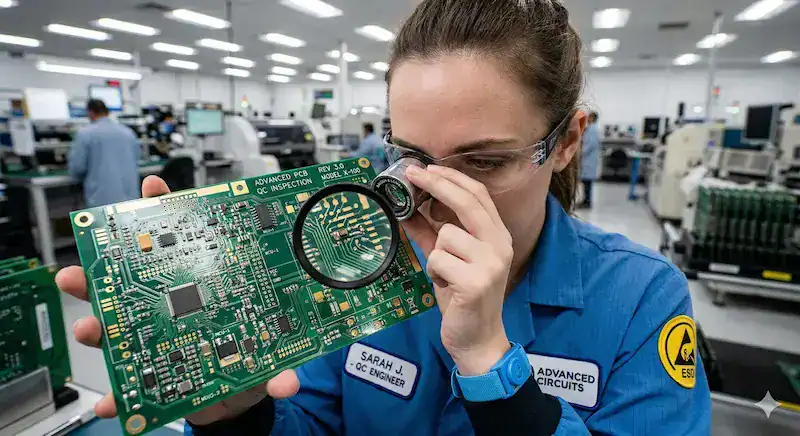
- Magnifier Inspection: Use a 10x loupe or a cheap digital microscope to inspect fine trace etching quality and mask alignment over BGA pads.
- Gerber Verification: Compare the physical silkscreen text and via placements against your original CAD files to catch old file version mix-ups.
If your boards fail this quick test, stop assembly immediately. We provide a free DFM/DFA engineering review on every order to prevent these exact headaches. Contact us today to get your free quote and see how a clean fabrication process works.
FAQ
Are minor scratches on the solder mask considered a defect? It depends on the depth. Light surface scuffs that do not expose the underlying copper are generally acceptable under IPC Class 2 standards. Deep scratches that reveal bare copper violate the standard because they create a high risk of solder bridging during assembly.
Can a warped PCB be fixed? Yes, but only if it is a bare board with minor bowing. The factory can bake the board at 105°C and press it flat under a heavy cold plate. If the board is already populated with components, you cannot flatten it without fracturing the solder joints.
How do I know if the factory messed up my impedance? The only way to know for sure is by asking the factory for a Time Domain Reflectometer (TDR) test report. Reputable manufacturers include an impedance test coupon on the production panel and measure it before shipping the boards to you.
Written by the QueenEMS Engineering Team