
Quick Answer: The right PCB copper weight depends entirely on your sustained current load. Standard 1oz copper easily handles up to 5A, while upgrading to 2oz or 3oz safely supports 20A to 50A but increases your bare board fabrication costs by 20% to 100%. Key takeaways:
- 1oz copper (35μm thick) covers 70% of all circuit board designs and is the most cost-effective standard.
- Specifying 2oz copper increases your fabrication price by 20% to 40% compared to 1oz.
- A 10mil trace routed on 1oz copper safely carries about 1A of current with a 10°C temperature rise.
- Thicker copper forces wider routing rules; a 3oz board requires absolute minimum trace widths of 8mil to 10mil.
- What is PCB copper weight and why does it matter?
- How do you choose between 1oz, 2oz, and 3oz copper?
- How does copper weight affect PCB fabrication cost?
- What happens when copper weight affects your trace width rules?
- Can you mix different copper weights on the same board?
- When should you consider heavy copper (3oz+)?
- FAQ
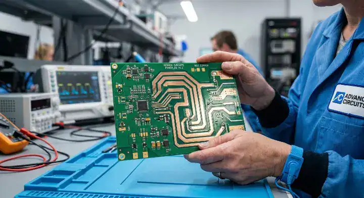
You are laying out a power delivery network for a new motor controller, staring at your CAD screen, wondering if you should bump the whole board up to 2oz copper just to be safe. Guessing wrong on this single specification costs you dearly. If you use 1oz copper for a 15A load, your traces will overheat and burn the FR4 material. If you blindly default to 2oz for a simple sensor board, you waste money and force your routing to be unnecessarily wide. After processing over 3,500 manufacturing orders last year, we built a simple framework for this exact decision. Here is how to map your current load to the exact copper thickness you need in under 30 seconds.
What is PCB copper weight and why does it matter?
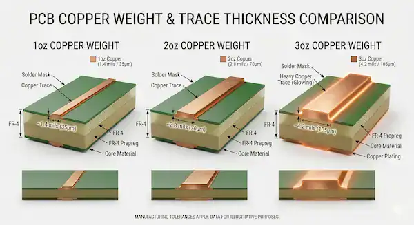
PCB copper weight measures the thickness of the copper foil on your board, with 1oz equaling exactly 35 micrometers (μm) thick. Upgrading to 2oz (70μm) or 3oz (105μm) doubles or triples your current carrying capacity without requiring you to draw wider physical traces on the board surface.
But here’s what most guides won’t tell you… heavy copper fundamentally changes your thermal management strategy. Standard digital signals do not care about copper thickness. You only need to increase your copper weight when you are pushing high amps or trying to dissipate extreme heat away from a power component.
Typical applications for different weights:
- 0.5oz to 1oz (18μm – 35μm): Standard digital logic, microcontrollers, and IoT sensor boards.
- 2oz (70μm): Moderate power supplies, DC-DC converters, and LED lighting arrays.
- 3oz (105μm): Battery management systems (BMS) and industrial equipment controllers.
How do you choose between 1oz, 2oz, and 3oz copper?
You can choose your PCB copper weight by matching it to your maximum sustained current; use 1oz for loads under 5A, switch to 2oz for currents between 5A and 20A, and specify 3oz for heavy loads up to 50A. As a baseline reference, a standard 10mil trace on 1oz copper safely carries about 1A with a 10°C temperature rise.
Here’s where it gets real… engineers constantly over-engineer their stackups. Over 70% of the boards we manufacture use standard 1oz copper because it is simply the best option for mixed-signal designs. If your board only handles data signals and low-power ICs, do not upgrade to 2oz.
Use this quick decision table to pick your thickness immediately:
| Maximum Sustained Current | Recommended PCB Copper Weight | Best Practice |
|---|---|---|
| ≤ 5A | 1 oz (35μm) | Use wide polygon pours for the power nets; keep traces fine. |
| 5A to 20A | 2 oz (70μm) | The sweet spot for standard power electronics. |
| 20A to 50A | 3 oz (105μm) | Requires careful thermal relief design on soldering pads. |
| > 50A | 4oz+ (Heavy Copper) | Move to specialized heavy copper PCB manufacturing. |
Upload your BOM and Gerber files to our portal for a free DFM check if you are unsure about your power routing. We will flag high-resistance choke points before you pay for manufacturing.
How does copper weight affect PCB fabrication cost?
Increasing your PCB copper weight from 1oz to 2oz raises your bare board fabrication cost by 20% to 40%, while jumping to 3oz adds a 50% to 100% premium. The raw copper material costs more, and the factory has to spend significantly more time etching the thicker metal in the chemical baths.
So what does this actually mean for your budget? The direct price premium is only half the story. Thick copper forces you to use wider trace spacing. Wider spacing means you cannot route components as tightly together, which forces you to increase the overall physical size of your board. Paying for a larger board compounds your total PCB fabrication cost quickly.
Here is a relative cost comparison for a standard 100×100mm, 2-layer FR4 board at a 100-piece volume:
| Copper Specification | Estimated Cost Impact | Manufacturing Lead Time |
|---|---|---|
| 1 oz / 1 oz | Base Price (100%) | Standard (3-5 days) |
| 2 oz / 2 oz | +20% to +40% | Standard |
| 3 oz / 3 oz | +50% to +100% | Adds 1-2 days |
What happens when copper weight affects your trace width rules?
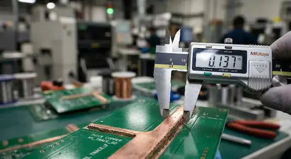
Specifying a heavier copper weight physically prevents you from routing fine traces, forcing your minimum trace width from 3mil on 1oz copper up to 8mil or 10mil on 3oz copper. The acid used in the etching process undercuts thick copper walls, meaning fine 4mil traces will simply wash away and break connections in the factory.
Now, here’s the part that surprises most customers… you cannot design a dense BGA processor board with 2oz copper. The escape routing under a fine-pitch chip requires 4mil lines, which are impossible to etch reliably on thick metal. Review our PCB trace width spacing guide to see how etch factors work.
If you choose a specific copper thickness, you must obey these minimum routing rules:
| Copper Weight | Absolute Minimum Trace Width | Absolute Minimum Spacing |
|---|---|---|
| 0.5 oz (Internal layers) | 3 mil | 3 mil |
| 1 oz | 3 mil to 4 mil | 3 mil to 4 mil |
| 2 oz | 5 mil to 6 mil | 5 mil to 6 mil |
| 3 oz | 8 mil to 10 mil | 8 mil to 10 mil |
Can you mix different copper weights on the same board?
Yes, you can mix different copper weights on different layers of the same board, but you must keep the distribution perfectly symmetrical relative to the center core. For example, if your top layer uses 2oz copper, your bottom layer must also use 2oz copper to prevent catastrophic thermal stress.
The real question is… what happens if you ignore symmetry? If you put 3oz copper on the top and 1oz on the bottom, the mismatched metals expand at drastically different rates inside the 260°C reflow oven. Read our factory breakdown on PCB warping causes to see how asymmetrical stackups destroy PCBA yield rates.
When should you consider heavy copper (3oz+)?
You should consider upgrading to heavy copper designs starting at 4oz and going up to 10oz when your circuit must carry continuous currents exceeding 50A. Instead of designing a massive, expensive 2-layer board with 6oz copper, you can usually save money by routing the power across a 4-layer board using 3oz copper on multiple layers.
Splitting your current across multiple inner layers improves heat distribution and keeps your external trace rules manageable. We cover this exact pricing strategy in our 2-layer vs 4-layer PCB comparison. For extremely demanding EV chargers or solar inverters, dive into our dedicated heavy copper PCB design handbook.
FAQ
Can I use 1oz copper for power traces if I just make them wider? Yes. If you have plenty of physical space on your board, pouring a massive 200mil wide polygon on 1oz copper can carry the same current as a narrow trace on 3oz copper. Always run your numbers through our PCB trace width calculator to verify the temperature rise.
Does 2oz copper improve signal integrity? No, thicker copper does not improve high-speed digital signal integrity. In fact, thicker traces increase the sidewall capacitance, which makes impedance control slightly more difficult to manufacture perfectly. Stick to 1oz or 0.5oz for high-speed routing.
Why does the factory use 0.5oz copper for internal layers? Internal layers are usually plated up during the via hole-wall metallization process. Starting with 0.5oz base foil allows the factory to plate the vias securely while bringing the final internal copper thickness up to a standard 1oz equivalent.
Written by the QueenEMS Engineering Team