
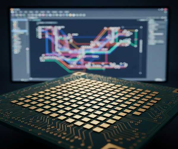
Successful BGA footprint design requires a meticulous balance of pad geometry, via placement, and layer stack-up to ensure signal integrity and high manufacturing yields.
Imagine you have just received a batch of high-density prototypes, only to find that the fine-pitch BGA components have shorts under the balls or, worse, open circuits that only appear under thermal stress. You spent weeks on the logical design, but the physical escape routing was so cramped that the manufacturer had to push the limits of their registration tolerances, resulting in a 30% yield loss. This frustration is common when the physical layout of the bga footprint is treated as an afterthought rather than a core engineering challenge. By mastering standardized escape methods and pad definitions early, you can eliminate these assembly nightmares and ensure a smooth transition from prototype to volume production.
Why Is the BGA Footprint Critical for Modern Layouts?
The bga footprint serves as the primary interface between complex integrated circuits and the PCB, dictating the routing density and the overall reliability of the solder joints.
How does ball pitch influence design?
As you move toward 0.5mm or 0.4mm pitches, the physical space available for traces and vias shrinks exponentially. This requires you to transition from standard routing to advanced high-density interconnect (HDI) strategies to maintain clearance.
- Pitch determines the maximum via size that can fit between pads.
- Smaller pitches often necessitate High-Density PCB Assembly Services to handle micro-vias.
But that’s just the beginning of the spatial puzzle.
Key Takeaway
Properly calculating ball pitch is the first step in determining whether your project requires standard or advanced manufacturing processes.
[Photorealism: A macro view of a high-density PCB showing a precise BGA footprint with micro-vias and fine-line routing.]
| Pitch (mm) | Technology Level | Typical Via Type |
| 1.0 – 0.8 | Standard | Through-hole |
| 0.65 – 0.5 | Advanced | Blind/Buried |
| < 0.5 | HDI | Via-in-pad |
Standardizing your pitch calculations early prevents costly late-stage layout revisions.
Should You Choose NSMD or SMD Pad Designs for BGA?
The bga footprint typically utilizes either Non-Solder Mask Defined (NSMD) or Solder Mask Defined (SMD) pads, each offering distinct advantages for mechanical strength and routing space.
What are the benefits of NSMD?
NSMD pads provide a smaller copper area, which gives you more room to route traces between the pads on the top layer. Because the solder mask is cleared away from the copper, the solder can wrap around the sides of the pad for a stronger metallurgical bond.
- NSMD is generally preferred for fine-pitch BGAs due to increased routing space.
- It offers better registration accuracy since copper etching is more precise than mask printing.
You might be wondering if SMD has a place in your design.
Key Takeaway
NSMD is the industry standard for high-density escaping, but it requires careful PCB Design for Manufacturing (DFM) Review to ensure pad adhesion.
[Photorealism: A technical comparison diagram showing the cross-section of an NSMD pad versus an SMD pad on a PCB.]
| Pad Type | Routing Space | Bond Strength | Best For |
| NSMD | High | Side-wetting | Fine Pitch |
| SMD | Low | Overlap | Ruggedized |
Selecting the right pad definition is a critical decision that impacts both signal integrity and assembly yield.
How Does Dogbone Routing Work for BGA Escaping?
Dogbone routing is the most common method used in a bga footprint to transition signals from the pads to internal layers using standard through-hole vias.
Is dogbone routing right for your pitch?
You use this technique by placing a via at the center of four pads and connecting it with a short “bone” trace. This works perfectly for 0.8mm pitches and above where there is sufficient clearance for mechanical drilling.
- It allows for lower-cost manufacturing compared to via-in-pad.
- This method is standard for Multi-Layer PCB Assembly in consumer electronics.
But what happens when the space disappears?
Key Takeaway
Dogbone routing is cost-effective but becomes physically impossible as component density increases and pitches shrink below 0.65mm.
[Photorealism: A top-down PCB layout view showing the “dogbone” via patterns radiating from a BGA center.]
| Feature | Dogbone Specs | Impact |
| Via Size | 0.2mm – 0.3mm | Mechanical Drill |
| Trace Width | 0.1mm – 0.125mm | Standard Etch |
| Layer Usage | High | Increases Stack-up |
Dogbone routing remains the baseline for reliable, mid-density BGA escaping.
When Is Via-in-Pad Necessary for BGA Footprints?
For ultra-fine pitch components, the bga footprint must often incorporate via-in-pad technology to save space and improve signal performance.
Why transition to via-in-pad?
You place the via directly inside the BGA pad, eliminating the “dogbone” trace and significantly increasing the available area for routing. This is essential for BGA Assembly and Rework Services where space is at a premium.
- Reduces parasitic inductance, which is vital for high-speed signals.
- Requires specialized “filling and capping” to prevent solder from wicking down the hole.
Believe it or not, the manufacturing cost increases are often offset by the reduced layer count.
Key Takeaway
Via-in-pad is the ultimate space-saving tool but requires a partner capable of advanced SMT Assembly Services to handle the plating.
[Photorealism: A 3D cross-section of a BGA solder ball sitting directly on a resin-filled and copper-capped micro-via.]
| Via-in-Pad Factor | Requirement | Purpose |
| Filling | Conductive/Non-conductive Epoxy | Prevent wicking |
| Capping | Copper Plating | Flat Solder Surface |
| Cost | +25% to +40% | Advanced Process |
Integrating via-in-pad technology can simplify complex routing but demands high-precision manufacturing.
How Do You Calculate the Required Layer Count?
The bga footprint complexity directly dictates the number of layers needed to escape all the signals without causing crosstalk or congestion.
Can you predict the stack-up?
You can estimate the layers by counting the number of signal rows in the BGA; typically, every two rows of pads require at least one signal layer for escaping. If you have an 8-row deep BGA, you are looking at a minimum of 4 signal layers just for the escape.
- High-speed signals may require interleaved ground planes for shielding.
- Power distribution often requires dedicated thick copper planes.
Does your current design follow these ratios?
Key Takeaway
Estimating layer count early in the bga footprint phase prevents budget overruns caused by adding layers late in the layout.
[Photorealism: A colorful diagram of a 12-layer PCB stack-up with BGA signals escaping on multiple internal layers.]
| BGA Rows | Signal Layers Needed | Complexity |
| 2 – 4 | 2 | Low |
| 6 – 8 | 4 | Moderate |
| 10+ | 6+ | High (HDI) |
Matching your stack-up to your BGA row depth is the key to an efficient and routable layout.
What Are the Best Practices for Power Plane Design?
In a bga footprint, the power and ground planes must be robust enough to handle high current loads while providing a stable reference for signal traces. +1
How do you optimize the PDN?
You should use solid planes whenever possible, but the forest of vias under a BGA often turns the planes into “Swiss cheese.” Designing the via pitch to allow for wide copper “bridges” between the holes is essential for maintaining low impedance.
- Place decoupling capacitors as close to the BGA pads as possible.
- Use wide planes for high-current rails to prevent voltage drops.
Could your power planes be causing your signal noise?
Key Takeaway
Optimizing your power distribution network (PDN) within the bga footprint is as important as the signal escape for high-performance chips.
[Photorealism: A heat-map visualization showing current density through a BGA power plane with via obstructions.]
| PDN Element | Design Rule | Result |
| Plane Integrity | Maximize copper bridges | Low Resistance |
| Capacitor Placement | Direct via connection | Low Inductance |
| Ground Reference | Continuous under signals | Low EMI |
A stable power network begins with a carefully designed via pattern under the BGA.
How to Handle High-Speed Differential Pairs in BGA?
Routing differential pairs through a bga footprint requires strict adherence to length matching and impedance control to avoid signal degradation.
Is symmetry the secret?
You must ensure that the escape vias for a differential pair are placed symmetrically and that the trace lengths are matched from the pad to the via. Any skew introduced here can cause common-mode noise that ruins your EMI performance.
- Keep pair traces close together to maintain consistent differential impedance.
- Avoid placing high-speed pairs near noisy power vias.
Are your pairs truly balanced?
Key Takeaway
High-speed escaping in a bga footprint demands a symmetry-first approach to preserve signal integrity for protocols like PCIe or DDR.
[Photorealism: A layout screenshot showing perfectly matched differential pairs zigzagging through a BGA via field.]
| High-Speed Metric | Target | Method |
| Impedance | 90 / 100 Ohms | Trace width/spacing |
| Skew | < 5 mils | Length matching |
| Crosstalk | < -30 dB | Increased spacing |
Symmetrical via placement is the foundation of high-speed differential signal integrity.
What Are the Clearance Constraints for BGA Routing?

The bga footprint must adhere to the manufacturer’s minimum trace-to-trace and trace-to-via clearances to prevent short circuits and production errors.
Can you push the limits safely?
You should aim for at least 3-4 mil traces and 3-4 mil spaces in dense areas, but always check with your assembly partner. Pushing below these limits often triggers the need for expensive SMT Assembly Services with high-precision imaging.
- Tighter clearances increase the risk of “copper slivers” during etching.
- Proper spacing prevents signal crosstalk in adjacent escape traces.
Do you know your manufacturer’s “sweet spot”?
Key Takeaway
Designing with manufacturing tolerances in mind for your bga footprint ensures your project remains cost-effective and reliable.
[Photorealism: A microscopic inspection image showing fine-line traces and the spacing between BGA escape vias.]
| Clearance Type | Minimum (mils) | Preferred (mils) |
| Trace-to-Pad | 3 | 4 |
| Trace-to-Trace | 3 | 5 |
| Via-to-Via | 5 | 8 |
Respecting clearance limits is the simplest way to improve your PCB assembly yield.
How to Optimize BGA Fanout for Manufacturing Yield?
The fanout strategy of your bga footprint should be designed to allow for easy inspection and cleaning during the assembly process.
Is your fanout “clean”?
You should avoid creating narrow channels or “acid traps” where manufacturing chemicals can become trapped. A clean, orthogonal fanout pattern not only looks better but also makes BGA Assembly and Rework Services much more straightforward.
- Use a “center-out” routing strategy to prevent congestion at the edges.
- Ensure ground vias are placed strategically to provide return paths for all signals.
Have you considered how a technician will rework this board?
Key Takeaway
A manufacturability-focused fanout in your bga footprint design reduces production stress and increases long-term field reliability.
[Photorealism: A clean, symmetrical PCB fanout pattern with ground-shielded vias and organized signal groups.]
| Fanout Rule | Benefit |
| Center-Out | Balanced density |
| Ground Stitching | EMI reduction |
| Orthogonal Routing | Easier inspection |
Clean fanout design is the hallmark of a professional high-speed PCB layout.
Why Is Thermal Management Critical for BGA Footprints?
Because the bga footprint sits directly under the heat source, the copper layout must assist in dissipating thermal energy away from the silicon. +1
Can your pads double as heat sinks?
You should utilize “thermal vias” or via-in-pad structures connected to internal ground planes to pull heat away from the component. Without this, the BGA can reach temperatures that cause solder joint fatigue or even board delamination.
- Thick internal copper planes act as thermal spreaders.
- Large via arrays help move heat to the bottom side of the PCB.
Is your device running too hot for its own good?
Key Takeaway
Integrating thermal dissipation paths into the bga footprint is essential for the longevity of high-power processors.
[Photorealism: A thermal camera image of a PCB with a central BGA, showing heat spreading through thermal vias to the ground plane.]
| Thermal Tool | Efficiency | Cost |
| Standard Vias | Moderate | Low |
| Via-in-Pad | High | Moderate |
| Copper Pours | High | Low |
A cool BGA is a reliable BGA, and it all starts with your copper layout.
Conclusion
Designing a robust bga footprint is the foundation of high-performance electronics, requiring a deep understanding of ball pitch, pad definition, and advanced routing techniques. By choosing between NSMD and SMD pads wisely and utilizing escape methods like dogbone or via-in-pad appropriately, you ensure both signal integrity and manufacturing success. We have addressed the critical pain points of layer optimization and clearance constraints to provide you with a clear path toward high-yield production.
Our engineering team specializes in transforming complex BGA designs into reliable hardware. Whether you need a simple 4-layer fanout or a high-density 12-layer HDI solution, we are here to help. Contact us today to review your next project and ensure your BGA layout is optimized for the future. We are your partner for excellence in Complex PCBA Solutions.
FAQ
Can I use through-hole vias for a 0.5mm pitch BGA?
It is extremely difficult. Standard mechanical drills usually can’t handle the small via sizes and tight clearances required for a 0.5mm pitch. In most cases, you must transition to micro-vias or via-in-pad technology, which typically requires a partner with High-Density PCB Assembly Services.
What is the best way to determine the trace width for BGA escaping?
You should start by calculating the “channel” space available between the BGA pads. Subtract your manufacturer’s minimum clearance from the pitch, and the remaining space is what you have for the trace. For a 1.0mm pitch, you usually have plenty of room for 5-6 mil traces, but for 0.5mm, you may be limited to 3 mil lines.
How do I prevent solder wicking in via-in-pad BGA designs?
You must specify that the vias be “filled and capped.” This process involves filling the micro-via with a non-conductive epoxy and then plating copper over the top to create a flat, solderable surface. Without this, the solder will flow down into the via during reflow, causing an “insufficient solder” defect.
What is the difference between “trace escape” and “fanout”?
These terms are often used interchangeably, but “fanout” usually refers to the pattern of vias used to move signals off the BGA pads, while “trace escape” refers to the actual routing of those signals to the rest of the PCB layers. Both are essential parts of a successful bga footprint strategy.
Why does BGA routing often require an even number of layers?
Most PCB manufacturers prefer even layer counts (4, 6, 8, etc.) to maintain board flatness during the lamination process. Since BGA routing often requires symmetric signal/plane pairs, an even stack-up naturally fits the engineering requirements for impedance control and mechanical stability.