
Quick Answer: A successful heavy copper PCB design requires calculating trace widths using IPC-2152 standards and maintaining perfect copper symmetry across all layers to prevent thermal warping. While standard 1oz boards handle low-power logic, upgrading to 4oz–6oz copper allows you to safely route 100A to 200A of continuous current within a tightly restricted physical footprint.
Key takeaways:
- IPC-2152 is mandatory for heavy copper calculations; inner layer traces must be de-rated by roughly 50%.
- Trace spacing increases with copper weight: 6oz copper requires at least 15-20mil clearance due to etching undercut.
- Asymmetric copper distribution causes thermal expansion warping that easily exceeds the 0.75% IPC limit.
- Via aspect ratios in thick copper boards typically must stay below 8:1 to allow proper chemical plating.
- What is heavy copper PCB and when do you need it?
- How do I choose the right copper weight for my design?
- How do I calculate trace width for heavy copper PCB?
- What are the design rules that change with heavy copper?
- How do I prevent warping in heavy copper PCB designs?
- Can I mix heavy copper and standard copper on the same board?
- How much does heavy copper PCB cost compared to standard?
- What should I tell my manufacturer before starting a heavy copper design?
- FAQ
You need to route 100 amps across a compact motor controller, but standard 1oz copper traces would physically melt under that load. If you blindly increase the copper weight without adjusting your mechanical spacing rules, the factory will either reject your files immediately or build a board that warps like a potato chip inside the reflow oven. After reviewing and manufacturing thousands of high-power layouts, we see these design failures hit our CAM department weekly. Here is the exact framework to calculate trace widths, set your clearance rules, and verify physical manufacturability before you submit your heavy copper PCB design to the factory.
What is heavy copper PCB and when do you need it?
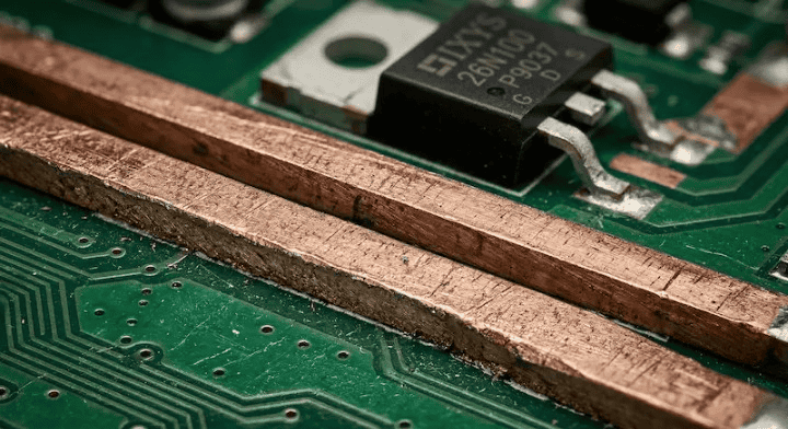
A heavy copper PCB features 3oz (105µm) to 20oz of copper weight per square foot, compared to the standard 1oz (35µm) thickness used in typical consumer electronics. You need this specialized fabrication when your board must carry extreme continuous currents, dissipate high localized heat loads without bulky external heatsinks, or survive repeated thermal cycling in harsh environments.
But here’s what most guides won’t tell you…
Heavy copper is not just about moving electricity; it functions as a built-in thermal management system. The thicker copper acts as a physical heat spreader, pulling heat away from high-power components like MOSFETs and IGBTs far more efficiently than standard FR4 material alone.
- High Current: Electric vehicle (EV) charging stations, industrial motor drives, and solar inverters.
- Thermal Management: High-power LED lighting arrays and server power supplies.
- Mechanical Strength: Designs requiring extreme physical resilience against thermal stress and mechanical bending.
2How do I choose the right copper weight for my design?
You choose the correct copper weight by balancing your target continuous current against your allowed temperature rise, the physical board space available for trace routing, and your project’s budget. Blindly selecting the thickest copper possible wastes money and massively complicates the chemical etching process.
Here’s where it gets real…
Engineers often struggle to pick a starting point. As a quick baseline reference: 4oz copper typically handles 50-100A, 6oz handles 100-200A, and 10oz+ is reserved for massive loads exceeding 500A per layer (assuming adequate trace widths).
To make the right decision, run your requirements through these four filters:
- Current Requirement: What is the absolute maximum continuous current?
- Space Limitations: If your board is physically small, you cannot route a 2-inch wide 1oz trace. You must increase the vertical copper thickness to reduce the horizontal trace width.
- Thermal Constraints: Thicker copper naturally lowers the resistance ($I^2R$ losses), keeping the board cooler.
- Cost Tolerance: Every time you step up a copper weight tier (e.g., from 3oz to 4oz), raw material and processing costs increase.
Table 1: Copper Weight Selection Reference Guide
| Copper Weight | Typical Current Range | Minimum Trace Width | Minimum Spacing | Typical Applications | Cost Impact |
|---|---|---|---|---|---|
| 1oz (35µm) | < 10A | 4mil | 4mil | Logic, standard MCU, low power | Baseline ($) |
| 3oz (105µm) | 20A – 50A | 8-10mil | 8-10mil | Power supplies, small motors | +20-40% |
| 4oz (140µm) | 50A – 100A | 12-15mil | 12-15mil | High-power amplifiers, converters | +50-80% |
| 6oz (210µm) | 100A – 200A | 15-20mil | 20mil+ | EV chargers, heavy robotics | +100% |
| 10oz+ (>350µm) | 500A+ | 30mil+ | 30mil+ | Industrial power distribution | Very High |
How do I calculate trace width for heavy copper PCB?
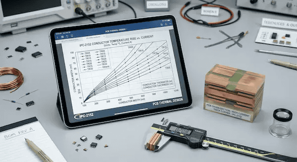
You must calculate heavy copper trace widths using the IPC-2152 standard, rather than the outdated IPC-2221, because IPC-2152 accurately accounts for how board thickness and copper weight actively pull heat away from the trace. Relying on older formulas will result in overly wide traces that waste valuable board real estate.
Now, here’s the part that surprises most customers…
Many ECAD tools still default to the old IPC-2221 calculators. If you are routing 3oz copper to carry 30A with an allowed temperature rise of 20°C, IPC-2152 will give you a significantly more accurate, often narrower trace width because it understands the thermal physics of the thick metal.
- Download and use the free Saturn PCB Toolkit; it is the industry standard for IPC-2152 math.
- Always de-rate inner layer traces by roughly 50%. A 3oz trace trapped inside FR4 cannot shed heat via convection like a 3oz trace sitting on the top surface.
- Factor in ambient temperature: If your board operates inside a hot sealed enclosure, your allowed temperature rise ($\Delta T$) is much smaller.
Table 2: Trace Calculation Standards: IPC-2221 vs IPC-2152
| Feature | IPC-2221 (Legacy) | IPC-2152 (Modern) |
|---|---|---|
| Release Year | 1998 (Based on 1950s data) | 2009 (Based on modern testing) |
| Accuracy | Very conservative | Highly accurate |
| Considers Copper Weight? | No | Yes |
| Considers Board Material? | No | Yes |
| Recommended For | Legacy low-power designs | Any heavy copper PCB design |
What are the design rules that change with heavy copper?
Upgrading to heavy copper requires fundamentally expanding your minimum trace spacing, increasing your minimum trace widths, enlarging component pad sizes, and restricting your via aspect ratios to account for aggressive chemical etching. You cannot apply standard 1oz Design Rule Check (DRC) parameters to a 4oz board.
The real question is…
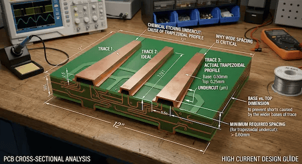
Do you understand how thick copper is actually made? The acid bath eats the copper horizontally at the same time it eats it vertically. This “undercut” means traces become trapezoidal. If you place two 6oz traces 5mils apart, the acid cannot fit between them to etch cleanly, resulting in a dead short.
- Trace Width & Spacing: 1oz copper supports 4/4mil (width/space). 3oz requires 8/8mil. 6oz demands 15/20mil minimums.
- Via Aspect Ratio: Plating thick copper inside a tiny hole is chemically difficult. Keep your via aspect ratio (board thickness to hole diameter) below 8:1.
- Pad Sizes: Increase pad sizes slightly. The massive thermal mass of heavy copper rapidly pulls heat away from the soldering iron or reflow oven, requiring larger landing areas to prevent cold joints.
Table 3: Standard vs Heavy Copper PCB Design Rules
| Rule Category | Standard (1oz) | Heavy (3oz) | Extreme Heavy (6oz) |
|---|---|---|---|
| Min Trace Width | 4mil | 8 – 10mil | 15 – 20mil |
| Min Trace Spacing | 4mil | 8 – 10mil | 20mil |
| Via Aspect Ratio Limits | 10:1 to 12:1 | 8:1 | 6:1 |
| Manufacturing Difficulty | Low | Medium | High |
How do I prevent warping in heavy copper PCB designs?
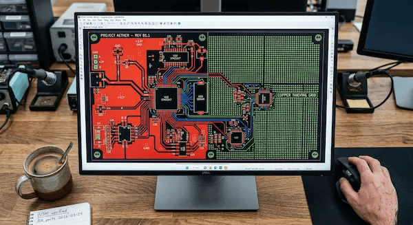
You prevent warping in a heavy copper PCB design by distributing the heavy copper symmetrically across the center axis of your layer stack-up and adding “copper thieving” (dummy copper pours) to empty areas to balance the metal density. Failing to balance the copper guarantees physical deformation during the high heat of lamination.
Want the honest answer?
Copper and FR4 fiberglass expand at completely different rates when heated. If you have a solid 4oz ground plane on Layer 1, and only a few signal traces on Layer 4, the board will literally bend toward the heavy copper side inside the reflow oven.
When a board bows or twists past the strict 0.75% IPC limit, the automated SMT pick-and-place machines will fail to drop parts accurately, leading directly to PCB prototype failure.
- The Z-Axis Symmetry Rule: Layer 1 must mirror Layer X. Layer 2 must mirror Layer X-1.
- Copper Thieving: Fill large blank spaces with isolated copper dots or cross-hatching to equalize the physical metal volume across the board’s surface.
- Work with your factory’s CAM team early; they use software to calculate copper density percentages per layer.
Can I mix heavy copper and standard copper on the same board?
Yes, you can mix heavy copper and standard copper on the same board using hybrid fabrication techniques like PowerLink or embedded copper coins. This allows you to route massive 10oz power lines for an inverter directly alongside fine-pitch 1oz traces for the sensitive microcontroller logic.
It all comes down to this…
If you try to route a 0.5mm pitch BGA chip on a 6oz copper layer, the required 20mil etching clearances make it geometrically impossible to break out the pins.
Hybrid construction saves money and space. Instead of building two separate boards and connecting them with heavy cables, the factory strategically plates thick copper only where the high-current paths reside. Keep in mind that this is an advanced manufacturing technique and carries a higher setup cost.
How much does heavy copper PCB cost compared to standard?
A 3oz heavy copper PCB typically increases your bare board costs by 20% to 40% compared to standard 1oz FR4, while massive 6oz or 10oz designs can easily double or triple your total fabrication expenses. The price jump comes from extended chemical etching times, specialized prepreg materials, and higher scrap rates.
So what does this actually mean for your budget?
Do not over-specify your copper. Every extra ounce adds direct material cost and limits your routing density. If you can achieve the necessary current capacity by routing a 2oz trace on the top layer and a parallel 2oz trace on the bottom layer, it is often cheaper than paying for a single 4oz layer.
When calculating your total PCB assembly cost, remember that heavy copper also requires more thermal energy during SMT reflow, occasionally increasing assembly fees due to custom thermal profiling.
What should I tell my manufacturer before starting a heavy copper design?
You must provide your manufacturer with your target copper weight, planned minimum trace width, minimum trace spacing, and via size requirements so their CAM engineers can confirm physical capability before you spend weeks routing the board. Waiting until the design is finished to ask questions guarantees painful re-work.
Here is the bottom line from the factory floor:
- The most common mistake engineers make on their first heavy copper layout is submitting files strictly using standard 1oz DRC rules. Every week, we reject high-current layouts because the trace spacing is too tight, the via aspect ratios are impossible to plate, or the copper distribution is horribly asymmetric.
- At QueenEMS turnkey assembly, we require all heavy copper orders to go through a rigorous capability pre-check. Before you lock in your layout, we verify your target copper weight against your minimum clearances and issue a comprehensive DFM PCB design report.
- By enforcing this strict pre-flight capability check, our heavy copper orders achieve a first-pass prototyping yield of over 92%, saving our customers an average of 10 to 14 days of frustrating back-and-forth design modifications.
FAQ
Can I hand-solder components onto a heavy copper PCB? It is extremely difficult. Heavy copper acts as a massive heatsink that pulls the heat away from your soldering iron faster than the iron can supply it. To hand-solder effectively, you usually need a high-wattage iron (80W+) and a pre-heating plate beneath the board to bring the entire assembly up to a baseline temperature before applying solder.
Why do my vias fail in heavy copper boards? Vias fail in thick boards because plating copper deep inside a narrow hole is difficult when the surrounding copper planes are very thick. If the aspect ratio (board thickness divided by hole diameter) is too high, the plating chemicals cannot circulate properly, resulting in thin, weak copper walls inside the via barrel that crack under thermal stress. Keep your aspect ratios low (e.g., 6:1).
Does heavy copper affect the solder mask application? Yes. Etching 4oz or 6oz copper leaves deep “valleys” between the traces. Standard liquid photoimageable (LPI) solder mask struggles to fill these deep gaps evenly without thinning out over the sharp top edges of the traces. Factories must apply multiple coats of solder mask or use specialized thick-film masks to ensure proper electrical isolation.
Preparing to start your heavy copper PCB design? Do not guess on the design rules. Before you export your files for a PCB assembly quote, contact the QueenEMS engineering team to verify your spacing and copper weight requirements. We provide a free capability review to ensure your board is physically buildable on the first try. Start your project at QueenEMS today.
Written by the QueenEMS Engineering Team