

Quick Answer: The decision between a 2 layer vs 4 layer PCB comes down to signal frequency, component density, and your budget. While a 4-layer board costs 30-80% more at Chinese factories, it provides dedicated ground and power planes that slash EMI and make routing high-density components like BGAs possible. Key takeaways:
- US factories charge 200-300% more for 4-layer boards, but Chinese fabs only charge 30-80% more.
- 2-layer boards fail FCC testing more frequently when handling signals above 50MHz.
- Upgrading to 4 layers adds 1-2 days to fabrication lead times due to the lamination process.
- Forcing high-density routing onto a 2-layer board increases assembly defects and raises your assembly costs.
- What’s the real difference between a 2 layer vs 4 layer PCB?
- How much more does a 4-layer PCB cost than a 2-layer?
- Does a 4-layer board take longer to manufacture?
- When is a 2-layer board the wrong choice?
- 5 questions to decide: 2 layer vs 4 layer PCB?
- When should you consider 6 layers or more?
- FAQ
You’re staring at your CAD tool, wondering if you can squeeze that Bluetooth module onto a double-sided board to save a few bucks. Your boss wants the cheapest unit price, but you know a noisy power supply might ruin the product’s performance. After processing 3,200+ PCB fabrication and assembly orders last year, we see engineers get stuck on the 2 layer vs 4 layer PCB debate constantly. Here is the exact data on costs, lead times, and routing density you need to make the right call today.
What’s the real difference between a 2 layer vs 4 layer PCB?
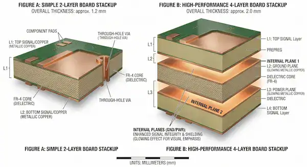
A 2-layer PCB routes all signals, power, and ground on just the top and bottom copper layers, whereas a 4-layer PCB adds two internal copper planes specifically for VCC and GND. This internal plane structure reduces electromagnetic interference (EMI) by up to 20dB compared to a 2-layer board.
But here’s what most guides won’t tell you… the physical stackup changes everything about how your signals behave. On a double-sided board, your return paths are messy and unpredictable. On a 4-layer board, your high-speed signals sit right next to a solid ground plane, creating a tight return path that prevents crosstalk.
If you want to understand the physics of complex layer counts, read our full guide on what is a multilayer PCB design. For most hardware startups, the difference boils down to this: 4-layer boards give you a massive routing playground, while 2-layer boards force you to compromise.
How much more does a 4-layer PCB cost than a 2-layer?
A 4-layer board typically costs 30% to 80% more than a 2-layer board when manufactured in China, compared to a 200% to 300% markup at US-based factories. The price gap is widest during the 5-piece prototype phase due to fixed setup fees, but it shrinks significantly at 100+ unit production volumes.
So what does this actually mean for your budget? Many engineers blindly trust outdated forums like Quora, where users claim 4-layer boards are “3 to 4 times more expensive.” That is only true if you manufacture locally in North America. At QueenEMS, our highly optimized supply chain means the jump to 4 layers won’t destroy your hardware budget.
Here is a realistic cost comparison for a standard 100×100mm FR4 board:
| Order Volume | 2-Layer PCB Estimate | 4-Layer PCB Estimate | The Real Difference |
|---|---|---|---|
| 5 pcs (Prototype) | $10 – $15 total | $30 – $45 total | Setup fees hit 4-layer harder |
| 100 pcs (Small Batch) | $0.80 – $1.20 / pc | $1.40 – $1.80 / pc | Only a 30-50% increase |
To see how surface finishes and copper weight impact these numbers, check out our complete breakdown on PCB fabrication cost.
Does a 4-layer board take longer to manufacture?
Yes, a 4-layer PCB takes 1 to 2 extra business days to fabricate because it requires an additional lamination cycle to bond the internal core and prepreg layers together. Standard 2-layer boards typically take 2-3 days, while standard 4-layer boards take 4-5 days.
Here’s the thing… this slight delay only affects the bare board fabrication. If your 2-layer board is overly complicated and crowded, it will slow down the entire assembly process later on. We offer free 2-4 layer FR4 prototypes for new customers through our rapid PCB prototyping service, so lead time shouldn’t be your primary bottleneck.
When is a 2-layer board the wrong choice?
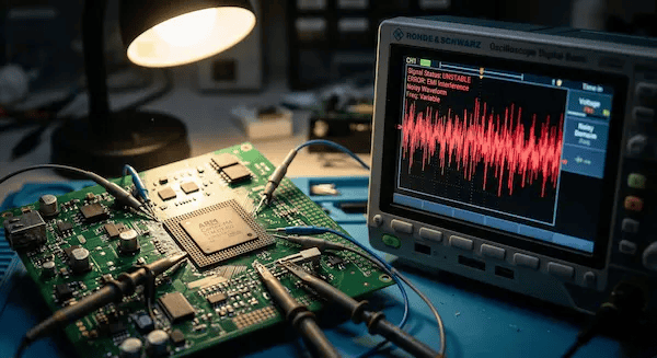
A 2-layer board is the wrong choice if your design features signal frequencies above 50MHz, relies on BGA or fine-pitch QFN packages, or requires strict EMC/FCC certification. Forcing complex routing onto two layers drops your surface mount yield rates and increases your overall PCB assembly cost.
Here’s where it gets real… 80% of first-time hardware startups try to force complex RF circuits onto double-sided boards to save money. Last year, a client designed a Bluetooth module on a 2-layer board. It functioned perfectly on the bench but failed FCC certification due to massive radiated emissions. We moved the design to a 4-layer stackup with a solid GND plane, and it passed on the first try. Saving that $200 on bare boards initially cost them over $3,000 in rework and re-testing delays.
Do not use a 2-layer board if:
- You are routing USB 2.0/3.0, SPI, or high-speed I2C lines.
- You have high-density packages like BGAs where escape routing requires internal layers.
- Your board area is highly restricted, leaving no room for power traces.
5 questions to decide: 2 layer vs 4 layer PCB?
You can decide between a 2 layer vs 4 layer PCB in two minutes by answering five simple yes-or-no questions about your signal speed, component pitch, and board dimensions. If you answer “yes” to any of the first four questions, you need a 4-layer board.
Want the honest answer? Skip the textbook physics and run your design through this quick checklist:
- Is your highest signal frequency over 50MHz? → Yes → 4-layer
- Does your BOM include BGA or fine-pitch QFN components? → Yes → 4-layer
- Does your product need to pass EMC/FCC certification? → Yes → 4-layer
- Is your board smaller than 50×50mm but holds more than 30 components? → Yes → 4-layer
- Did you answer “no” to everything above? → 2-layer is fine.
If you are still unsure, do not guess. Upload your Gerber files to our team for a free DFM engineering review, and we will tell you exactly what your circuit requires.
When should you consider 6 layers or more?
You should upgrade to a 6-layer or 8-layer PCB when your design includes DDR memory routing, multiple high-speed impedance-controlled traces, or more than three distinct power voltage domains. A 6-layer board provides the extra routing layers needed to isolate sensitive analog signals from noisy digital buses.
For simple microcontrollers and sensor boards, 4 layers give you the best performance-to-cost ratio. When you step into the world of application processors, FPGAs, and dense telecommunications equipment, you will need a dedicated multilayer PCB manufacturer who can handle 6 to 60 layers with strict impedance control.
FAQ
Can I route high-speed USB on a 2-layer board? No, you shouldn’t. While it might function over very short distances, maintaining the required 90-ohm differential impedance is incredibly difficult without a solid reference plane directly below the traces. Use a 4-layer board to avoid data drops.
Is a 4-layer board thicker than a 2-layer board? It depends, but usually no. The standard thickness for both 2-layer and 4-layer boards is 1.6mm (0.062 inches). The manufacturer simply uses thinner internal cores and prepreg materials to fit four copper layers into the same overall thickness.
How do I test if my 4-layer prototype works before mass production? You should build a small batch first. Upload your BOM and Gerbers to QueenEMS for a free DFM review. We provide full turnkey service from component sourcing to final testing, complete with 3D AOI and X-Ray inspection on every BGA joint.
Written by the QueenEMS Engineering Team